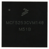
MCF5253CVM140 Freescale Semiconductor, MCF5253CVM140 Datasheet - Page 40

MCF5253CVM140
Manufacturer Part Number
MCF5253CVM140
Description
IC MPU 32BIT 140MHZ 225-MAPBGA
Manufacturer
Freescale Semiconductor
Series
MCF525xr
Datasheets
1.MCF5253VM140J.pdf
(34 pages)
2.MCF5253VM140J.pdf
(8 pages)
3.MCF5253VM140J.pdf
(648 pages)
4.MCF5253VM140J.pdf
(2 pages)
Specifications of MCF5253CVM140
Core Processor
Coldfire V2
Core Size
32-Bit
Speed
140MHz
Connectivity
CAN, EBI/EMI, I²C, QSPI, UART/USART, USB OTG
Peripherals
DMA, WDT
Program Memory Type
ROMless
Ram Size
128K x 8
Voltage - Supply (vcc/vdd)
1.08 V ~ 1.32 V
Data Converters
A/D 6x12b
Oscillator Type
External
Operating Temperature
-40°C ~ 85°C
Package / Case
225-MAPBGA
Family Name
MCF5xxx
Device Core
ColdFire V2
Device Core Size
32b
Frequency (max)
140MHz
Instruction Set Architecture
RISC
Supply Voltage 1 (typ)
1.2/3.3V
Operating Supply Voltage (max)
1.32/3.6V
Operating Supply Voltage (min)
1.08/3V
Operating Temp Range
-40C to 85C
Operating Temperature Classification
Industrial
Mounting
Surface Mount
Pin Count
225
Package Type
MA-BGA
Lead Free Status / RoHS Status
Lead free / RoHS Compliant
Number Of I /o
-
Eeprom Size
-
Program Memory Size
-
Lead Free Status / Rohs Status
Compliant
Available stocks
Company
Part Number
Manufacturer
Quantity
Price
Company:
Part Number:
MCF5253CVM140
Manufacturer:
FREESCALE
Quantity:
300
Company:
Part Number:
MCF5253CVM140
Manufacturer:
Freescale Semiconductor
Quantity:
10 000
Part Number:
MCF5253CVM140
Manufacturer:
FREESCALE
Quantity:
20 000
Company:
Part Number:
MCF5253CVM140J
Manufacturer:
Freescale Semiconductor
Quantity:
10 000
- MCF5253VM140J PDF datasheet
- MCF5253VM140J PDF datasheet #2
- MCF5253VM140J PDF datasheet #3
- MCF5253VM140J PDF datasheet #4
- Current page: 40 of 648
- Download datasheet (8Mb)
MCF5253 Introduction
1.5.4
The instruction cache improves system performance by providing cached instructions to the execution unit
in a single clock cycle. The MCF5253 processor uses an 8K-byte, direct-mapped instruction cache to
achieve 125 MIPS at 140 MHz. The cache is accessed by physical addresses, where each 16-byte line
consists of an address tag and a valid bit. The instruction cache also includes a bursting interface for 16-bit
and 8-bit port sizes to quickly fill cache lines.
1.5.5
The 128-Kbyte on-chip SRAM is split over two banks, SRAM0 (64K) and SRAM1 (64K). It provides
single clock-cycle access for the ColdFire core. This SRAM can store processor stack and critical code or
data segments to maximize performance. Memory in the second bank (SRAM1) can be accessed under
DMA.
1.5.6
The MCF5253 DRAM controller provides a glueless interface for one bank of DRAM, and can address up
to 32MB. The controller supports a 16-bit data bus. The controller operates in page mode, non-page mode,
and burst-page mode and supports SDRAMs.
1.5.7
The MCF5253 provides a glueless interface to 16-bit port size SRAM, ROM, and peripheral devices with
independent programmable control of the assertion and negation of chip-select and write-enable signals.
The MCF5253 also supports bursting ROMs.
1.5.8
The bus interface controller transfers data between the ColdFire core or DMA and memory, peripherals,
or other devices on the external bus. The external bus interface provides 23 address lines, a 16-bit data bus,
Output Enable, and Read/Write signals. This interface implements an extended synchronous protocol that
supports bursting operations.
1.5.9
The USB module in the MCF5253 is used for communication to a PC or communication to slave devices,
e.g. to download data from a hard disc player to a flash player, to a photo printer and so on. The USB
supports full Host mode functionality. The USB supports the OTG supplement to the USB 2.0
specification. It operates as high speed, full speed and low speed host, and as high speed and full speed
device. Host negotiation protocol (HNP) and session request protocol (SRP) are implemented with
software support.
A USB 2.0 high-speed compatible PHY is integrated on-chip.
1-8
Instruction Cache
Internal 128-Kbyte SRAM
DRAM Controller
System Interface
External Bus Interface
USB 2.0 High-Speed On-The-Go
MCF5253 Reference Manual, Rev. 1
Freescale Semiconductor
Related parts for MCF5253CVM140
Image
Part Number
Description
Manufacturer
Datasheet
Request
R
Part Number:
Description:
Mcf5253 Coldfire? Microprocessor Data Sheet
Manufacturer:
Freescale Semiconductor, Inc
Datasheet:
Part Number:
Description:
Manufacturer:
Freescale Semiconductor, Inc
Datasheet:
Part Number:
Description:
Manufacturer:
Freescale Semiconductor, Inc
Datasheet:
Part Number:
Description:
Manufacturer:
Freescale Semiconductor, Inc
Datasheet:
Part Number:
Description:
Manufacturer:
Freescale Semiconductor, Inc
Datasheet:
Part Number:
Description:
Manufacturer:
Freescale Semiconductor, Inc
Datasheet:
Part Number:
Description:
Manufacturer:
Freescale Semiconductor, Inc
Datasheet:
Part Number:
Description:
Manufacturer:
Freescale Semiconductor, Inc
Datasheet:
Part Number:
Description:
Manufacturer:
Freescale Semiconductor, Inc
Datasheet:
Part Number:
Description:
Manufacturer:
Freescale Semiconductor, Inc
Datasheet:
Part Number:
Description:
Manufacturer:
Freescale Semiconductor, Inc
Datasheet:
Part Number:
Description:
Manufacturer:
Freescale Semiconductor, Inc
Datasheet:
Part Number:
Description:
Manufacturer:
Freescale Semiconductor, Inc
Datasheet:
Part Number:
Description:
Manufacturer:
Freescale Semiconductor, Inc
Datasheet:
Part Number:
Description:
Manufacturer:
Freescale Semiconductor, Inc
Datasheet:


