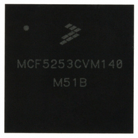
MCF5253CVM140 Freescale Semiconductor, MCF5253CVM140 Datasheet - Page 172

MCF5253CVM140
Manufacturer Part Number
MCF5253CVM140
Description
IC MPU 32BIT 140MHZ 225-MAPBGA
Manufacturer
Freescale Semiconductor
Series
MCF525xr
Datasheets
1.MCF5253VM140J.pdf
(34 pages)
2.MCF5253VM140J.pdf
(8 pages)
3.MCF5253VM140J.pdf
(648 pages)
4.MCF5253VM140J.pdf
(2 pages)
Specifications of MCF5253CVM140
Core Processor
Coldfire V2
Core Size
32-Bit
Speed
140MHz
Connectivity
CAN, EBI/EMI, I²C, QSPI, UART/USART, USB OTG
Peripherals
DMA, WDT
Program Memory Type
ROMless
Ram Size
128K x 8
Voltage - Supply (vcc/vdd)
1.08 V ~ 1.32 V
Data Converters
A/D 6x12b
Oscillator Type
External
Operating Temperature
-40°C ~ 85°C
Package / Case
225-MAPBGA
Family Name
MCF5xxx
Device Core
ColdFire V2
Device Core Size
32b
Frequency (max)
140MHz
Instruction Set Architecture
RISC
Supply Voltage 1 (typ)
1.2/3.3V
Operating Supply Voltage (max)
1.32/3.6V
Operating Supply Voltage (min)
1.08/3V
Operating Temp Range
-40C to 85C
Operating Temperature Classification
Industrial
Mounting
Surface Mount
Pin Count
225
Package Type
MA-BGA
Lead Free Status / RoHS Status
Lead free / RoHS Compliant
Number Of I /o
-
Eeprom Size
-
Program Memory Size
-
Lead Free Status / Rohs Status
Compliant
Available stocks
Company
Part Number
Manufacturer
Quantity
Price
Company:
Part Number:
MCF5253CVM140
Manufacturer:
FREESCALE
Quantity:
300
Company:
Part Number:
MCF5253CVM140
Manufacturer:
Freescale Semiconductor
Quantity:
10 000
Part Number:
MCF5253CVM140
Manufacturer:
FREESCALE
Quantity:
20 000
Company:
Part Number:
MCF5253CVM140J
Manufacturer:
Freescale Semiconductor
Quantity:
10 000
- MCF5253VM140J PDF datasheet
- MCF5253VM140J PDF datasheet #2
- MCF5253VM140J PDF datasheet #3
- MCF5253VM140J PDF datasheet #4
- Current page: 172 of 648
- Download datasheet (8Mb)
System Integration Module (SIM)
At power-on, the function is always the primary function. When a ‘0’ is programmed in any bit of
GPIO-FUNCTION or GPIO1-FUNCTION, the corresponding pin gets its primary function. In this case,
output drive strength and output value are determined by the primary function logic. When a ‘1’ is
programmed the corresponding pin is in GPO-mode, drive direction is determined by value in GPIO-EN
or GPIO1-EN. When a ‘0’ is programmed in any bit, the corresponding pin is driven to high-impedance
state. When a ‘1’ is programmed, the corresponding pin is driven low or high.
When a pin is in GPO-mode, and being driven low-impedance, the actual drive value of the pin is
determined by what is programmed in the corresponding bit of registers GPIO-OUT or GPIO1-OUT. If
‘0’ is programmed here, the pin is driven low. If ‘1’ is programmed, the pin is driven high.
9-28
GPIO-Function
Bit Number
GPIO-OUT
GPIO-EN
31
30
29
28
27
26
25
24
23
22
21
20
19
18
17
QSPIDOUT/SFSY/GPIO27
QSPICS2/MCLK2/GPIO24
SDATAO1/TOUT0/GPIO18
QSPICLK/SUBR/GPIO25
CS1/QSPICS3/GPIO28
RCK/QSPIDIN/QSPI
Table 9-29. General-Purpose Output Register Bits to Pins Mapping
IDE_DIOR/GPIO31
BUFENB2/GPIO30
BUFENB1/GPIO29
WAKEUP/GPIO21
SDATAI1/GPIO17
Associated Pin
LRCK2/GPIO23
LRCK1/GPIO19
SCLK2/GPIO22
SCLK1/GPIO20
Figure 9-15. General-Purpose Pin Logic for Pin SCLK3/GPIO35
DOUT/GPIO26
SCLK3 Drive Strength
GPIO1-FUNCTION
SCLK3 Drive Value
SCLK3 Input Value
GPIO1-READ
GPIO1-OUT
GPIO1-EN
MCF5253 Reference Manual, Rev. 1
Pin Type
I/O
I/O
I/O
I/O
I/O
I/O
I/O
I/O
I/O
I/O
I/O
I/O
I/O
I/O
I/O
0
1
0
1
GPIO1-Function
GPIO1-OUT
Bit Number
GPIO1-EN
59
57
56
63
62
61
60
58
55
54
53
52
51
50
49
SCLK3/GPIO35
ADOUT/SCLK4/GPIO58
SDUDQM/GPO53
SD_CS0/GPIO60
SDLDQM/GPO52
PSTCLK/GPIO51
SDRAS/GPIO59
Associated Pin
BCLKE/GPIO63
PST0/GPIO50
PST1/GPIO49
A23/GPO54
none
none
none
none
none
Freescale Semiconductor
Pin Type
I/O
I/O
I/O
I/O
I/O
I/O
I/O
I/O
I/O
I/O
I/O
I/O
O
O
O
Related parts for MCF5253CVM140
Image
Part Number
Description
Manufacturer
Datasheet
Request
R
Part Number:
Description:
Mcf5253 Coldfire? Microprocessor Data Sheet
Manufacturer:
Freescale Semiconductor, Inc
Datasheet:
Part Number:
Description:
Manufacturer:
Freescale Semiconductor, Inc
Datasheet:
Part Number:
Description:
Manufacturer:
Freescale Semiconductor, Inc
Datasheet:
Part Number:
Description:
Manufacturer:
Freescale Semiconductor, Inc
Datasheet:
Part Number:
Description:
Manufacturer:
Freescale Semiconductor, Inc
Datasheet:
Part Number:
Description:
Manufacturer:
Freescale Semiconductor, Inc
Datasheet:
Part Number:
Description:
Manufacturer:
Freescale Semiconductor, Inc
Datasheet:
Part Number:
Description:
Manufacturer:
Freescale Semiconductor, Inc
Datasheet:
Part Number:
Description:
Manufacturer:
Freescale Semiconductor, Inc
Datasheet:
Part Number:
Description:
Manufacturer:
Freescale Semiconductor, Inc
Datasheet:
Part Number:
Description:
Manufacturer:
Freescale Semiconductor, Inc
Datasheet:
Part Number:
Description:
Manufacturer:
Freescale Semiconductor, Inc
Datasheet:
Part Number:
Description:
Manufacturer:
Freescale Semiconductor, Inc
Datasheet:
Part Number:
Description:
Manufacturer:
Freescale Semiconductor, Inc
Datasheet:
Part Number:
Description:
Manufacturer:
Freescale Semiconductor, Inc
Datasheet:


