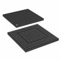
MPC8308VMAGD Freescale Semiconductor, MPC8308VMAGD Datasheet - Page 894

MPC8308VMAGD
Manufacturer Part Number
MPC8308VMAGD
Description
MPU POWERQUICC II PRO 473MAPBGA
Manufacturer
Freescale Semiconductor
Datasheets
1.MPC8308VMAGD.pdf
(90 pages)
2.MPC8308VMAGD.pdf
(2 pages)
3.MPC8308VMAGD.pdf
(1170 pages)
4.MPC8308VMAGD.pdf
(14 pages)
Specifications of MPC8308VMAGD
Processor Type
MPC83xx PowerQUICC II Pro 32-Bit
Speed
400MHz
Voltage
1V
Mounting Type
Surface Mount
Package / Case
473-MAPBGA
Product
Network Processor
Data Rate
256 bps
Frequency
400 MHz
Supply Voltage (max)
3.6 V
Supply Voltage (min)
3 V
Supply Current (max)
5 uA
Maximum Operating Temperature
+ 105 C
Minimum Operating Temperature
0 C
Interface
I2C, JTAG, SPI
Mounting Style
SMD/SMT
Lead Free Status / RoHS Status
Lead free / RoHS Compliant
Features
-
Lead Free Status / Rohs Status
Lead free / RoHS Compliant
Available stocks
Company
Part Number
Manufacturer
Quantity
Price
Company:
Part Number:
MPC8308VMAGD
Manufacturer:
FREESCAL
Quantity:
300
Company:
Part Number:
MPC8308VMAGD
Manufacturer:
Freescale Semiconductor
Quantity:
10 000
Part Number:
MPC8308VMAGD
Manufacturer:
FREESCALE
Quantity:
20 000
Company:
Part Number:
MPC8308VMAGD400/266
Manufacturer:
FREESCAL
Quantity:
300
Company:
Part Number:
MPC8308VMAGDA
Manufacturer:
Freescale Semiconductor
Quantity:
10 000
- MPC8308VMAGD PDF datasheet
- MPC8308VMAGD PDF datasheet #2
- MPC8308VMAGD PDF datasheet #3
- MPC8308VMAGD PDF datasheet #4
- Current page: 894 of 1170
- Download datasheet (9Mb)
Enhanced Three-Speed Ethernet Controllers
The eTSEC device is programmed by a combination of control/status registers (CSRs) and buffer
descriptors. The CSRs are used for mode control, interrupts, and to extract status information. The
descriptors are used to pass data buffers and related buffer status or frame information between the
hardware and software.
All accesses to and from the registers must be made as 32-bit accesses. There is no support for accesses of
sizes other than 32 bits. Writes to reserved register bits must always store 0, as writing 1 to reserved bits
may have unintended side-effects. Reads from unmapped register addresses return zero. Unless otherwise
specified, the read value of reserved bits in mapped registers is not defined, and must not be assumed to
be 0.
This section of the document defines the memory map and describes the registers in detail. The buffer
descriptor is described in
16.5.1
Each of the eTSECs is allocated 4 Kbytes of memory-mapped space. The space for each eTSEC is divided
as indicated in
16.5.2
The eTSEC memory mapped registers are accessed by reading and writing to an address comprised of the
base address (specified in IMMRBAR as defined in
address, plus the offset of the specific register to be accessed. Note that all memory-mapped registers must
only be accessed as 32-bit quantities.
Table 16-4
offsets to the memory map table are applicable to each eTSEC. Block base addresses are as follows:
16-10
•
•
eTSEC1 starts at 0x2_4000 address offset
eTSEC2 starts at 0x2_5000 address offset
lists the offset, name, and a cross-reference to the complete description of each register. The
Top-Level Module Memory Map
Detailed Memory Map
Table
16-3.
MPC8308 PowerQUICC II Pro Processor Reference Manual, Rev. 0
Section 16.6.7, “Buffer Descriptors.”
Address Offset
C40–DFF
A00–AFF
B00–BFF
C00–C3F
E00–EFF
000–0FF
100–2FF
300–4FF
500–5FF
600–7FF
800–8FF
900–9FF
Table 16-3. Module Memory Map Summary
eTSEC general control/status registers
eTSEC transmit control/status registers
eTSEC receive control/status registers
MAC registers
RMON MIB registers
Hash table registers
—
FIFO control/status registers
DMA system registers
Lossless Flow Control registers
—
1588 Hardware Assist
Chapter 3, “Memory
Function
Map.”) plus the block base
Freescale Semiconductor
Related parts for MPC8308VMAGD
Image
Part Number
Description
Manufacturer
Datasheet
Request
R
Part Number:
Description:
Development Boards & Kits - Other Processors MPC8308-NSG
Manufacturer:
Freescale Semiconductor
Datasheet:

Part Number:
Description:
MCU, MPU & DSP Development Tools For MPC8308 Ethernet USB I2C SPI
Manufacturer:
Freescale Semiconductor
Datasheet:

Part Number:
Description:
MCU, MPU & DSP Development Tools For MPC8308 Ethernet USB 32bit
Manufacturer:
Freescale Semiconductor
Datasheet:
Part Number:
Description:
Mpc8308 Powerquicc Ii Pro Processor Hardware Specification
Manufacturer:
Freescale Semiconductor, Inc
Datasheet:

Part Number:
Description:
BOARD REF DESIGN MPC8308
Manufacturer:
Freescale Semiconductor
Datasheet:

Part Number:
Description:
MPC8308 PowerQUICC II Pro Processor Hardware Specification
Manufacturer:
FREESCALE [Freescale Semiconductor, Inc]
Datasheet:
Part Number:
Description:
Microprocessors - MPU E300 ext tmp Qual266
Manufacturer:
Freescale Semiconductor
Datasheet:
Part Number:
Description:
Microprocessors - MPU E300 ext tmp Qual333
Manufacturer:
Freescale Semiconductor
Datasheet:
Part Number:
Description:
Microprocessors - MPU E300 EXT TEMP PB 400
Manufacturer:
Freescale Semiconductor
Datasheet:
Part Number:
Description:
Microprocessors - MPU E300 MP Pb 266
Manufacturer:
Freescale Semiconductor
Datasheet:
Part Number:
Description:
Microprocessors - MPU E300 MP Pb 400
Manufacturer:
Freescale Semiconductor
Datasheet:
Part Number:
Description:
Microprocessors - MPU E300 MP Pb 333
Manufacturer:
Freescale Semiconductor
Datasheet:
Part Number:
Description:
Manufacturer:
Freescale Semiconductor, Inc
Datasheet:
Part Number:
Description:
Manufacturer:
Freescale Semiconductor, Inc
Datasheet:
Part Number:
Description:
Manufacturer:
Freescale Semiconductor, Inc
Datasheet:


