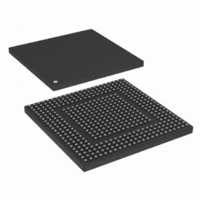
MPC8308VMAGD Freescale Semiconductor, MPC8308VMAGD Datasheet - Page 803

MPC8308VMAGD
Manufacturer Part Number
MPC8308VMAGD
Description
MPU POWERQUICC II PRO 473MAPBGA
Manufacturer
Freescale Semiconductor
Datasheets
1.MPC8308VMAGD.pdf
(90 pages)
2.MPC8308VMAGD.pdf
(2 pages)
3.MPC8308VMAGD.pdf
(1170 pages)
4.MPC8308VMAGD.pdf
(14 pages)
Specifications of MPC8308VMAGD
Processor Type
MPC83xx PowerQUICC II Pro 32-Bit
Speed
400MHz
Voltage
1V
Mounting Type
Surface Mount
Package / Case
473-MAPBGA
Product
Network Processor
Data Rate
256 bps
Frequency
400 MHz
Supply Voltage (max)
3.6 V
Supply Voltage (min)
3 V
Supply Current (max)
5 uA
Maximum Operating Temperature
+ 105 C
Minimum Operating Temperature
0 C
Interface
I2C, JTAG, SPI
Mounting Style
SMD/SMT
Lead Free Status / RoHS Status
Lead free / RoHS Compliant
Features
-
Lead Free Status / Rohs Status
Lead free / RoHS Compliant
Available stocks
Company
Part Number
Manufacturer
Quantity
Price
Company:
Part Number:
MPC8308VMAGD
Manufacturer:
FREESCAL
Quantity:
300
Company:
Part Number:
MPC8308VMAGD
Manufacturer:
Freescale Semiconductor
Quantity:
10 000
Part Number:
MPC8308VMAGD
Manufacturer:
FREESCALE
Quantity:
20 000
Company:
Part Number:
MPC8308VMAGD400/266
Manufacturer:
FREESCAL
Quantity:
300
Company:
Part Number:
MPC8308VMAGDA
Manufacturer:
Freescale Semiconductor
Quantity:
10 000
- MPC8308VMAGD PDF datasheet
- MPC8308VMAGD PDF datasheet #2
- MPC8308VMAGD PDF datasheet #3
- MPC8308VMAGD PDF datasheet #4
- Current page: 803 of 1170
- Download datasheet (9Mb)
Table 14-77
14.4.6.4
The PCI Express controller core clock ratio register, shown in
of the actual PCI Express controller core clock (csb_clk divided according to SCCR[PCIEXPnCM])
frequency to the maximum possible controller core frequency (125 MHz). Changing the default value of
this register is required only when a PCI Express controller core clock frequency is different than its
maximum.
This ratio will be used by the PCI Express controller only to calculate the actual timer values to be used
for Ack Latency and Replay timeout values. These two timer values have to dynamically change based on
the negotiated link-width and max-payload size. The default value by itself is not enough for these two
timers. By programming the clock ratio in this register, the calculation is automatically adjusted by
hardware. Note that other timer registers in the PCI Express controller may still have to be programmed
to a new value based on the actual controller core clock used in the specific application.
Freescale Semiconductor
31–27
26–13
12–0
Bits
ACKRTV
ACKLTV
Name
—
describes PCI Express N_FTS control register fields.
PCI Express Controller Core Clock Ratio Register (PEX_GCLK_RATIO
The default PCI Express controller core clock is csb_clk
(SCCR[PCIEXPnCM] = 0b01).
Table 14-77. PCI Express ACK Replay Timeout Register Fields Description
Reserved
Ack Replay Timeout Value. Timeout value to wait for reception of ACK DLLP from the link side by
the DLL before re-transmitting TLPs. The protocol specifies this value in symbol times for various
combinations of max-payload size and negotiated link width. The value programmed into this field
should be in terms of system clock cycles number, and can be calculated as:
Note: The “250” denominator represent the frequency of a symbol (250 MHz).
Ack Latency Timeout Value. Timeout value to force transmission of ACK DLLP by the DLL after a
TLP is received. The protocol specifies this value in symbol times for various combinations of
max-payload size & negotiated link width. The value programmed into this field should be in terms of
system clock cycles number, and can be calculated as:
Note: The “250” denominator represent the frequency of a symbol (250 MHz).
• REPLAY_TIMER_TIMEOUT—Timeout value for the replay timer, specified in symbol times.
• Rx_L0s_Adjustment—The time required by the component’s receive circuits to exit from L0s to L0
• SYSTEM_CLOCK—The PCI Express controller system clock, specified in MHz.
• ACK_LATENCY_TIMEOUT—Timeout value to force transmission of ACK DLLP, specified in symbol
• Tx_L0s_Adjustment—The time required for the Transmitter to exit L0s, specified in symbol times.
• SYSTEM_CLOCK—The PCI Express controller system clock, specified in MHz.
specified in symbol times.
times.
MPC8308 PowerQUICC II Pro Processor Reference Manual, Rev. 0
(
-------------------------------------------------------------------------------------------------------------------------------------------------------------------------------------------- -
(
------------------------------------------------------------------------------------------------------------------------------------------------------------------------------------------- -
REPLAY_TIMER_TIMEOUT
ACK_LATENCY_TIEMOUT
NOTE
Description
+
+
Rx_L0s_Adjustment
Tx_L0s_Adjustment
250
250
Figure
14-80, is used to program the ratio
)
)
×
×
SYSTEM_CLOCK
SYSTEM_CLOCK
PCI Express Interface Controller
14-65
)
Related parts for MPC8308VMAGD
Image
Part Number
Description
Manufacturer
Datasheet
Request
R
Part Number:
Description:
Development Boards & Kits - Other Processors MPC8308-NSG
Manufacturer:
Freescale Semiconductor
Datasheet:

Part Number:
Description:
MCU, MPU & DSP Development Tools For MPC8308 Ethernet USB I2C SPI
Manufacturer:
Freescale Semiconductor
Datasheet:

Part Number:
Description:
MCU, MPU & DSP Development Tools For MPC8308 Ethernet USB 32bit
Manufacturer:
Freescale Semiconductor
Datasheet:
Part Number:
Description:
Mpc8308 Powerquicc Ii Pro Processor Hardware Specification
Manufacturer:
Freescale Semiconductor, Inc
Datasheet:

Part Number:
Description:
BOARD REF DESIGN MPC8308
Manufacturer:
Freescale Semiconductor
Datasheet:

Part Number:
Description:
MPC8308 PowerQUICC II Pro Processor Hardware Specification
Manufacturer:
FREESCALE [Freescale Semiconductor, Inc]
Datasheet:
Part Number:
Description:
Microprocessors - MPU E300 ext tmp Qual266
Manufacturer:
Freescale Semiconductor
Datasheet:
Part Number:
Description:
Microprocessors - MPU E300 ext tmp Qual333
Manufacturer:
Freescale Semiconductor
Datasheet:
Part Number:
Description:
Microprocessors - MPU E300 EXT TEMP PB 400
Manufacturer:
Freescale Semiconductor
Datasheet:
Part Number:
Description:
Microprocessors - MPU E300 MP Pb 266
Manufacturer:
Freescale Semiconductor
Datasheet:
Part Number:
Description:
Microprocessors - MPU E300 MP Pb 400
Manufacturer:
Freescale Semiconductor
Datasheet:
Part Number:
Description:
Microprocessors - MPU E300 MP Pb 333
Manufacturer:
Freescale Semiconductor
Datasheet:
Part Number:
Description:
Manufacturer:
Freescale Semiconductor, Inc
Datasheet:
Part Number:
Description:
Manufacturer:
Freescale Semiconductor, Inc
Datasheet:
Part Number:
Description:
Manufacturer:
Freescale Semiconductor, Inc
Datasheet:


