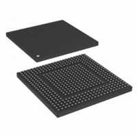
MPC8308VMAGD Freescale Semiconductor, MPC8308VMAGD Datasheet - Page 77

MPC8308VMAGD
Manufacturer Part Number
MPC8308VMAGD
Description
MPU POWERQUICC II PRO 473MAPBGA
Manufacturer
Freescale Semiconductor
Datasheets
1.MPC8308VMAGD.pdf
(90 pages)
2.MPC8308VMAGD.pdf
(2 pages)
3.MPC8308VMAGD.pdf
(1170 pages)
4.MPC8308VMAGD.pdf
(14 pages)
Specifications of MPC8308VMAGD
Processor Type
MPC83xx PowerQUICC II Pro 32-Bit
Speed
400MHz
Voltage
1V
Mounting Type
Surface Mount
Package / Case
473-MAPBGA
Product
Network Processor
Data Rate
256 bps
Frequency
400 MHz
Supply Voltage (max)
3.6 V
Supply Voltage (min)
3 V
Supply Current (max)
5 uA
Maximum Operating Temperature
+ 105 C
Minimum Operating Temperature
0 C
Interface
I2C, JTAG, SPI
Mounting Style
SMD/SMT
Lead Free Status / RoHS Status
Lead free / RoHS Compliant
Features
-
Lead Free Status / Rohs Status
Lead free / RoHS Compliant
Available stocks
Company
Part Number
Manufacturer
Quantity
Price
Company:
Part Number:
MPC8308VMAGD
Manufacturer:
FREESCAL
Quantity:
300
Company:
Part Number:
MPC8308VMAGD
Manufacturer:
Freescale Semiconductor
Quantity:
10 000
Part Number:
MPC8308VMAGD
Manufacturer:
FREESCALE
Quantity:
20 000
Company:
Part Number:
MPC8308VMAGD400/266
Manufacturer:
FREESCAL
Quantity:
300
Company:
Part Number:
MPC8308VMAGDA
Manufacturer:
Freescale Semiconductor
Quantity:
10 000
- MPC8308VMAGD PDF datasheet
- MPC8308VMAGD PDF datasheet #2
- MPC8308VMAGD PDF datasheet #3
- MPC8308VMAGD PDF datasheet #4
- Current page: 77 of 1170
- Download datasheet (9Mb)
such, it supports a minimal glue logic interface to SRAM, EPROM, NOR Flash EPROM, NAND Flash
EPROM, Flash EPROM, burstable RAM, and other peripherals.
The eLBC also includes a number of data checking and protection features such as data parity generation
and checking, write protection, and a bus monitor to ensure that each bus cycle is terminated within a
user-specified period.
The eLBC provides two Write Enable signals to allow single-byte write access to external 16-bit eLBC
slave devices.
The main features of the enhanced local bus controller (eLBC) are as follows:
Freescale Semiconductor
•
•
•
Memory controller with four memory banks (chip selects)
— 32-bit address decoding with mask
— Variable memory block sizes (32 Kbytes to 2 Gbytes in FCM mode, 32 Kbytes to 64 Mbytes
— Selection of control signal generation on a per-bank basis
— Data buffer controls activated on a per-bank basis
— Up to 256-byte bursts, arbitrarily aligned
— Automatic segmentation of large transactions into memory accesses optimized for bus width
— Write-protection capability
— Atomic operation
General-purpose chip-select machine (GPCM)
— Compatible with SRAM, EPROM, NOR Flash EEPROM, FEPROM, and peripherals
— Global (boot) chip-select available at system reset
— Boot chip-select support for 8- and 16-bit devices
— Minimum three-clock access to external devices
— Two byte-write-enable signals (LWE[0:1])
— Output enable signal (LOE)
— External access termination signal (LGTA)
NAND Flash control machine (FCM)
— Compatible with small (512 + 16 bytes) and large (2048 + 64 bytes) page parallel NAND
— Global (boot) chip-select available at system reset, with 4-Kbyte boot block buffer for
— Boot chip-select support for 8-bit devices
— Dual 2-Kbyte/eight 512-byte buffers allow simultaneous data transfer during Flash reads and
— Interrupt-driven block transfer for reads and writes
— Programmable command and data transfer sequences of up to eight steps supported
— Generic command and address registers support proprietary Flash interfaces
in UPM mode, and 32 Kbytes to 64 Mbytes in GPCM mode)
and addressing capability
Flash EEPROM
execute-in-place boot loading
programming
MPC8308 PowerQUICC II Pro Processor Reference Manual, Rev. 0
Overview
1-13
Related parts for MPC8308VMAGD
Image
Part Number
Description
Manufacturer
Datasheet
Request
R
Part Number:
Description:
Development Boards & Kits - Other Processors MPC8308-NSG
Manufacturer:
Freescale Semiconductor
Datasheet:

Part Number:
Description:
MCU, MPU & DSP Development Tools For MPC8308 Ethernet USB I2C SPI
Manufacturer:
Freescale Semiconductor
Datasheet:

Part Number:
Description:
MCU, MPU & DSP Development Tools For MPC8308 Ethernet USB 32bit
Manufacturer:
Freescale Semiconductor
Datasheet:
Part Number:
Description:
Mpc8308 Powerquicc Ii Pro Processor Hardware Specification
Manufacturer:
Freescale Semiconductor, Inc
Datasheet:

Part Number:
Description:
BOARD REF DESIGN MPC8308
Manufacturer:
Freescale Semiconductor
Datasheet:

Part Number:
Description:
MPC8308 PowerQUICC II Pro Processor Hardware Specification
Manufacturer:
FREESCALE [Freescale Semiconductor, Inc]
Datasheet:
Part Number:
Description:
Microprocessors - MPU E300 ext tmp Qual266
Manufacturer:
Freescale Semiconductor
Datasheet:
Part Number:
Description:
Microprocessors - MPU E300 ext tmp Qual333
Manufacturer:
Freescale Semiconductor
Datasheet:
Part Number:
Description:
Microprocessors - MPU E300 EXT TEMP PB 400
Manufacturer:
Freescale Semiconductor
Datasheet:
Part Number:
Description:
Microprocessors - MPU E300 MP Pb 266
Manufacturer:
Freescale Semiconductor
Datasheet:
Part Number:
Description:
Microprocessors - MPU E300 MP Pb 400
Manufacturer:
Freescale Semiconductor
Datasheet:
Part Number:
Description:
Microprocessors - MPU E300 MP Pb 333
Manufacturer:
Freescale Semiconductor
Datasheet:
Part Number:
Description:
Manufacturer:
Freescale Semiconductor, Inc
Datasheet:
Part Number:
Description:
Manufacturer:
Freescale Semiconductor, Inc
Datasheet:
Part Number:
Description:
Manufacturer:
Freescale Semiconductor, Inc
Datasheet:


