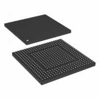
MPC8308VMAGD Freescale Semiconductor, MPC8308VMAGD Datasheet - Page 818

MPC8308VMAGD
Manufacturer Part Number
MPC8308VMAGD
Description
MPU POWERQUICC II PRO 473MAPBGA
Manufacturer
Freescale Semiconductor
Datasheets
1.MPC8308VMAGD.pdf
(90 pages)
2.MPC8308VMAGD.pdf
(2 pages)
3.MPC8308VMAGD.pdf
(1170 pages)
4.MPC8308VMAGD.pdf
(14 pages)
Specifications of MPC8308VMAGD
Processor Type
MPC83xx PowerQUICC II Pro 32-Bit
Speed
400MHz
Voltage
1V
Mounting Type
Surface Mount
Package / Case
473-MAPBGA
Product
Network Processor
Data Rate
256 bps
Frequency
400 MHz
Supply Voltage (max)
3.6 V
Supply Voltage (min)
3 V
Supply Current (max)
5 uA
Maximum Operating Temperature
+ 105 C
Minimum Operating Temperature
0 C
Interface
I2C, JTAG, SPI
Mounting Style
SMD/SMT
Lead Free Status / RoHS Status
Lead free / RoHS Compliant
Features
-
Lead Free Status / Rohs Status
Lead free / RoHS Compliant
Available stocks
Company
Part Number
Manufacturer
Quantity
Price
Company:
Part Number:
MPC8308VMAGD
Manufacturer:
FREESCAL
Quantity:
300
Company:
Part Number:
MPC8308VMAGD
Manufacturer:
Freescale Semiconductor
Quantity:
10 000
Part Number:
MPC8308VMAGD
Manufacturer:
FREESCALE
Quantity:
20 000
Company:
Part Number:
MPC8308VMAGD400/266
Manufacturer:
FREESCAL
Quantity:
300
Company:
Part Number:
MPC8308VMAGDA
Manufacturer:
Freescale Semiconductor
Quantity:
10 000
- MPC8308VMAGD PDF datasheet
- MPC8308VMAGD PDF datasheet #2
- MPC8308VMAGD PDF datasheet #3
- MPC8308VMAGD PDF datasheet #4
- Current page: 818 of 1170
- Download datasheet (9Mb)
PCI Express Interface Controller
14.5.3.1
PEX_CSB_OBCTRL, shown in
Table 14-96
14-80
Offset 0x840
Reset
Reset
31–10
Bits
9–7
6–4
3
2
1
0
W
W
R
R
31
15
MEMWE
CFGWE
Name
IOWE
PIOE
TC
—
—
defines the bit fields for PEX_CSB_OBCTRL.
Figure 14-98. PCI Express Outbound PIO Control Register (PEX_CSB_OBCTRL)
PCI Express Outbound PIO Control Register (PEX_CSB_OBCTRL)
Reserved
Traffic class. Indicates TC value to be used for TLP generation corresponding to traffic received by the
CSB slave.
Reserved
Configuration window enable. Must be set to enable an outbound configuration transaction. Indicates that
a CSB transactions directed to an outbound window can be mapped to Config write and read TLPs and
transmitted to the PCI Express link.
I/O window enable. Must be set to enable an outbound I/O transaction. Indicates that a CSB transactions
directed to an outbound window can be mapped to I/O write and read TLPs and transmitted to the
PCI Express link.
Memory window enable. Must be set to enable an outbound Memory transaction. Indicates that a CSB
transactions directed to an outbound window can be mapped to Memory write and read TLPs and
transmitted to the PCI Express link.
PIO enable. Must be set to enable an outbound PIO transaction. This field controls the general enable of
the PCI Express CSB bridge outbound PIO operation and should be set together with the other window
enable fields in this register.
—
Table 14-96. PEX_CSB_OBCTRL Register Fields Description
MPC8308 PowerQUICC II Pro Processor Reference Manual, Rev. 0
Figure
10
14-98, controls the PCI Express Outbound PIO operations.
9
TC
8
All zeros
All zeros
7
—
Description
6
—
4
CFGWE IOWE MEMWE PIOE
3
Freescale Semiconductor
2
Access: Read/Write
1
16
0
Related parts for MPC8308VMAGD
Image
Part Number
Description
Manufacturer
Datasheet
Request
R
Part Number:
Description:
Development Boards & Kits - Other Processors MPC8308-NSG
Manufacturer:
Freescale Semiconductor
Datasheet:

Part Number:
Description:
MCU, MPU & DSP Development Tools For MPC8308 Ethernet USB I2C SPI
Manufacturer:
Freescale Semiconductor
Datasheet:

Part Number:
Description:
MCU, MPU & DSP Development Tools For MPC8308 Ethernet USB 32bit
Manufacturer:
Freescale Semiconductor
Datasheet:
Part Number:
Description:
Mpc8308 Powerquicc Ii Pro Processor Hardware Specification
Manufacturer:
Freescale Semiconductor, Inc
Datasheet:

Part Number:
Description:
BOARD REF DESIGN MPC8308
Manufacturer:
Freescale Semiconductor
Datasheet:

Part Number:
Description:
MPC8308 PowerQUICC II Pro Processor Hardware Specification
Manufacturer:
FREESCALE [Freescale Semiconductor, Inc]
Datasheet:
Part Number:
Description:
Microprocessors - MPU E300 ext tmp Qual266
Manufacturer:
Freescale Semiconductor
Datasheet:
Part Number:
Description:
Microprocessors - MPU E300 ext tmp Qual333
Manufacturer:
Freescale Semiconductor
Datasheet:
Part Number:
Description:
Microprocessors - MPU E300 EXT TEMP PB 400
Manufacturer:
Freescale Semiconductor
Datasheet:
Part Number:
Description:
Microprocessors - MPU E300 MP Pb 266
Manufacturer:
Freescale Semiconductor
Datasheet:
Part Number:
Description:
Microprocessors - MPU E300 MP Pb 400
Manufacturer:
Freescale Semiconductor
Datasheet:
Part Number:
Description:
Microprocessors - MPU E300 MP Pb 333
Manufacturer:
Freescale Semiconductor
Datasheet:
Part Number:
Description:
Manufacturer:
Freescale Semiconductor, Inc
Datasheet:
Part Number:
Description:
Manufacturer:
Freescale Semiconductor, Inc
Datasheet:
Part Number:
Description:
Manufacturer:
Freescale Semiconductor, Inc
Datasheet:


