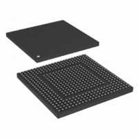
MPC8308VMAGD Freescale Semiconductor, MPC8308VMAGD Datasheet - Page 456

MPC8308VMAGD
Manufacturer Part Number
MPC8308VMAGD
Description
MPU POWERQUICC II PRO 473MAPBGA
Manufacturer
Freescale Semiconductor
Datasheets
1.MPC8308VMAGD.pdf
(90 pages)
2.MPC8308VMAGD.pdf
(2 pages)
3.MPC8308VMAGD.pdf
(1170 pages)
4.MPC8308VMAGD.pdf
(14 pages)
Specifications of MPC8308VMAGD
Processor Type
MPC83xx PowerQUICC II Pro 32-Bit
Speed
400MHz
Voltage
1V
Mounting Type
Surface Mount
Package / Case
473-MAPBGA
Product
Network Processor
Data Rate
256 bps
Frequency
400 MHz
Supply Voltage (max)
3.6 V
Supply Voltage (min)
3 V
Supply Current (max)
5 uA
Maximum Operating Temperature
+ 105 C
Minimum Operating Temperature
0 C
Interface
I2C, JTAG, SPI
Mounting Style
SMD/SMT
Lead Free Status / RoHS Status
Lead free / RoHS Compliant
Features
-
Lead Free Status / Rohs Status
Lead free / RoHS Compliant
Available stocks
Company
Part Number
Manufacturer
Quantity
Price
Company:
Part Number:
MPC8308VMAGD
Manufacturer:
FREESCAL
Quantity:
300
Company:
Part Number:
MPC8308VMAGD
Manufacturer:
Freescale Semiconductor
Quantity:
10 000
Part Number:
MPC8308VMAGD
Manufacturer:
FREESCALE
Quantity:
20 000
Company:
Part Number:
MPC8308VMAGD400/266
Manufacturer:
FREESCAL
Quantity:
300
Company:
Part Number:
MPC8308VMAGDA
Manufacturer:
Freescale Semiconductor
Quantity:
10 000
- MPC8308VMAGD PDF datasheet
- MPC8308VMAGD PDF datasheet #2
- MPC8308VMAGD PDF datasheet #3
- MPC8308VMAGD PDF datasheet #4
- Current page: 456 of 1170
- Download datasheet (9Mb)
Enhanced Local Bus Controller
10-76
10–11
22–23
Bits
12
13
14
15
16
17
18
19
20
21
G4T3/WAEN General purpose line 4 timing 3/wait enable. Bit function is determined by M x MR[GPL4].
G4T1/DLT3 General purpose line 4 timing 1/delay time 3. The function of this bit is determined by
REDO
Name
G1T1
G1T3
G2T1
G2T3
G3T1
G3T3
G5T1
G5T3
G0H
General purpose line 0 higher. Defines the state of LGPL0 during the bus clock quarter phases
3 and 4 (second half phase).
00 Value defined by M x MR[G0CL]
01 Reserved
10 0
11 1
General purpose line 1 timing 1. Defines the state (0 or 1) of LGPL1 during bus clock quarter
phases 1 and 2 (first half phase).
General purpose line 1 timing 3. Defines the state (0 or 1) of LGPL1 during bus clock quarter
phases 3 and 4 (second half phase)
General purpose line 2 timing 1. Defines state (0 or 1) of LGPL2 during bus clock quarter
phases 1 and 2 (first half phase).
General purpose line 2 timing 3. Defines the state (0 or 1) of LGPL2 during bus clock quarter
phases 3 and 4 (second half phase).
General purpose line 3 timing 1. Defines the state (0 or 1) of LGPL3 during bus clock quarter
phases 1 and 2 (first half phase).
General purpose line 3 timing 3. Defines the state (0 or 1) of LGPL3 during bus clock quarter
phases 3 and 4 (second half phase).
M x MR[GPL4].
If M x MR[GPL4] = 0 and LGPL4/LUPWAIT pin functions as an output (LGPL4), G4T1/DLT3
defines the state (0 or 1) of LGPL4 during bus clock quarter phases 1 and 2 (first half phase).
If M x MR[GPL4] = 1 and LGPL4/LUPWAIT functions as an input (LUPWAIT), if a read burst or
single read is executed, G4T1/DLT3 defines the sampling of the data bus as follows:
0 In the current word, the data bus should be sampled at the start of bus clock quarter phase
1 In the current word, the data bus should be sampled at the start of bus clock quarter phase
If M x MR[GPL4] = 0 and LGPL4/LUPWAIT pin functions as an output (LGPL4), G4T3/WAEN
defines the state (0 or 1) of LGPL4 during bus clock quarter phases 3 and 4 (second half phase).
If M x MR[GPL4] = 1 and LGPL4/LUPWAIT functions as an input (LUPWAIT), G4T3/WAEN is
used to enable the wait mechanism:
0 LUPWAIT detection is disabled.
1 LUPWAIT is enabled. If LUPWAIT is detected as being asserted, a freeze in the external
General purpose line 5 timing 1. Defines the state (0 or 1) of LGPL5 during bus clock quarter
phases 1 and 2 (first half phase).
General purpose line 5 timing 3. Defines the state (0 or 1) of LGPL5 during bus clock quarter
phases 3 and 4 (second half phase).
Redo current RAM word. Defines the number of times to execute the current RAM word.
00 Once (normal operation)
01 Twice
10 Three times
11 Four times
MPC8308 PowerQUICC II Pro Processor Reference Manual, Rev. 0
1 of the next bus clock cycle.
3 of the current bus clock cycle.
signals logical values occurs until LUPWAIT is detected as being negated.
Table 10-40. RAM Word Field Descriptions (continued)
Description
Freescale Semiconductor
Related parts for MPC8308VMAGD
Image
Part Number
Description
Manufacturer
Datasheet
Request
R
Part Number:
Description:
Development Boards & Kits - Other Processors MPC8308-NSG
Manufacturer:
Freescale Semiconductor
Datasheet:

Part Number:
Description:
MCU, MPU & DSP Development Tools For MPC8308 Ethernet USB I2C SPI
Manufacturer:
Freescale Semiconductor
Datasheet:

Part Number:
Description:
MCU, MPU & DSP Development Tools For MPC8308 Ethernet USB 32bit
Manufacturer:
Freescale Semiconductor
Datasheet:
Part Number:
Description:
Mpc8308 Powerquicc Ii Pro Processor Hardware Specification
Manufacturer:
Freescale Semiconductor, Inc
Datasheet:

Part Number:
Description:
BOARD REF DESIGN MPC8308
Manufacturer:
Freescale Semiconductor
Datasheet:

Part Number:
Description:
MPC8308 PowerQUICC II Pro Processor Hardware Specification
Manufacturer:
FREESCALE [Freescale Semiconductor, Inc]
Datasheet:
Part Number:
Description:
Microprocessors - MPU E300 ext tmp Qual266
Manufacturer:
Freescale Semiconductor
Datasheet:
Part Number:
Description:
Microprocessors - MPU E300 ext tmp Qual333
Manufacturer:
Freescale Semiconductor
Datasheet:
Part Number:
Description:
Microprocessors - MPU E300 EXT TEMP PB 400
Manufacturer:
Freescale Semiconductor
Datasheet:
Part Number:
Description:
Microprocessors - MPU E300 MP Pb 266
Manufacturer:
Freescale Semiconductor
Datasheet:
Part Number:
Description:
Microprocessors - MPU E300 MP Pb 400
Manufacturer:
Freescale Semiconductor
Datasheet:
Part Number:
Description:
Microprocessors - MPU E300 MP Pb 333
Manufacturer:
Freescale Semiconductor
Datasheet:
Part Number:
Description:
Manufacturer:
Freescale Semiconductor, Inc
Datasheet:
Part Number:
Description:
Manufacturer:
Freescale Semiconductor, Inc
Datasheet:
Part Number:
Description:
Manufacturer:
Freescale Semiconductor, Inc
Datasheet:


