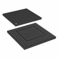
MPC8308VMAGD Freescale Semiconductor, MPC8308VMAGD Datasheet - Page 459

MPC8308VMAGD
Manufacturer Part Number
MPC8308VMAGD
Description
MPU POWERQUICC II PRO 473MAPBGA
Manufacturer
Freescale Semiconductor
Datasheets
1.MPC8308VMAGD.pdf
(90 pages)
2.MPC8308VMAGD.pdf
(2 pages)
3.MPC8308VMAGD.pdf
(1170 pages)
4.MPC8308VMAGD.pdf
(14 pages)
Specifications of MPC8308VMAGD
Processor Type
MPC83xx PowerQUICC II Pro 32-Bit
Speed
400MHz
Voltage
1V
Mounting Type
Surface Mount
Package / Case
473-MAPBGA
Product
Network Processor
Data Rate
256 bps
Frequency
400 MHz
Supply Voltage (max)
3.6 V
Supply Voltage (min)
3 V
Supply Current (max)
5 uA
Maximum Operating Temperature
+ 105 C
Minimum Operating Temperature
0 C
Interface
I2C, JTAG, SPI
Mounting Style
SMD/SMT
Lead Free Status / RoHS Status
Lead free / RoHS Compliant
Features
-
Lead Free Status / Rohs Status
Lead free / RoHS Compliant
Available stocks
Company
Part Number
Manufacturer
Quantity
Price
Company:
Part Number:
MPC8308VMAGD
Manufacturer:
FREESCAL
Quantity:
300
Company:
Part Number:
MPC8308VMAGD
Manufacturer:
Freescale Semiconductor
Quantity:
10 000
Part Number:
MPC8308VMAGD
Manufacturer:
FREESCALE
Quantity:
20 000
Company:
Part Number:
MPC8308VMAGD400/266
Manufacturer:
FREESCAL
Quantity:
300
Company:
Part Number:
MPC8308VMAGDA
Manufacturer:
Freescale Semiconductor
Quantity:
10 000
- MPC8308VMAGD PDF datasheet
- MPC8308VMAGD PDF datasheet #2
- MPC8308VMAGD PDF datasheet #3
- MPC8308VMAGD PDF datasheet #4
- Current page: 459 of 1170
- Download datasheet (9Mb)
The uppermost byte select (LBS0), when asserted, indicates that LD[0:7] contains valid data during a
cycle. Likewise, LBS1 indicates that LD[8:15] contain valid data. For a UPM refresh timer request, all
LBS[0:1] signals are asserted/negated by the UPM according to the refresh pattern only. Following any
internal bus monitor exception, the LBS[0:1] signals are negated regardless of the exception handling
provided by any UPM exception pattern to prevent spurious writes to external RAM.
10.4.4.4.4
The general-purpose signals (LGPL[0:5]) each have two bits in the RAM word that define the logical value
of the signal to be changed at the rising edge of the bus clock and/or at the falling edge of the bus clock.
LGPL0 offers enhancements beyond the other LGPLn lines.
LGPL0 can be controlled by an address line specified in MxMR[G0CL]. To use this feature, G0H and G0L
should be set in the RAM word. For example, for a SIMM with multiple banks, this address line can be
used to switch between internal memory device banks.
10.4.4.4.5
The LOOP bit in the RAM word specifies the beginning and end of a set of UPM RAM words that are to
be repeated. The first time LOOP = 1, the memory controller recognizes it as a loop start word and loads
the memory loop counter with the corresponding contents of the loop field shown in
RAM word for which LOOP = 1 is recognized as a loop end word. When it is reached, the loop counter is
decremented by one.
Continued loop execution depends on the loop counter. If the counter is not zero, the next RAM word
executed is the loop start word. Otherwise, the next RAM word executed is the one after the loop end word.
Loops can be executed sequentially but cannot be nested.
Also, special care must be taken that LAST and LOOP must not be set together.
10.4.4.4.6
The REDO function is useful for wait-state insertion in a long UPM routine that would otherwise need too
many RAM words. Setting the REDO bits of the RAM word to a nonzero value causes the UPM to
re-execute the current RAM word up to three more times, as defined in the REDO field of the current RAM
word.
Special care must be taken in the following cases:
Freescale Semiconductor
General-Purpose Signals (G n T n , GO n )
Loop Control (LOOP)
Repeat Execution of Current RAM Word (REDO)
Read single-beat cycle
Read burst cycle
Write single-beat cycle
Write burst cycle
Refresh timer expired
RUN command
MPC8308 PowerQUICC II Pro Processor Reference Manual, Rev. 0
Request Serviced
Table 10-41. M x MR Loop Field Use
Loop Field
WLF
WLF
RLF
RLF
RLF
TLF
Enhanced Local Bus Controller
Table
10-41. The next
10-79
Related parts for MPC8308VMAGD
Image
Part Number
Description
Manufacturer
Datasheet
Request
R
Part Number:
Description:
Development Boards & Kits - Other Processors MPC8308-NSG
Manufacturer:
Freescale Semiconductor
Datasheet:

Part Number:
Description:
MCU, MPU & DSP Development Tools For MPC8308 Ethernet USB I2C SPI
Manufacturer:
Freescale Semiconductor
Datasheet:

Part Number:
Description:
MCU, MPU & DSP Development Tools For MPC8308 Ethernet USB 32bit
Manufacturer:
Freescale Semiconductor
Datasheet:
Part Number:
Description:
Mpc8308 Powerquicc Ii Pro Processor Hardware Specification
Manufacturer:
Freescale Semiconductor, Inc
Datasheet:

Part Number:
Description:
BOARD REF DESIGN MPC8308
Manufacturer:
Freescale Semiconductor
Datasheet:

Part Number:
Description:
MPC8308 PowerQUICC II Pro Processor Hardware Specification
Manufacturer:
FREESCALE [Freescale Semiconductor, Inc]
Datasheet:
Part Number:
Description:
Microprocessors - MPU E300 ext tmp Qual266
Manufacturer:
Freescale Semiconductor
Datasheet:
Part Number:
Description:
Microprocessors - MPU E300 ext tmp Qual333
Manufacturer:
Freescale Semiconductor
Datasheet:
Part Number:
Description:
Microprocessors - MPU E300 EXT TEMP PB 400
Manufacturer:
Freescale Semiconductor
Datasheet:
Part Number:
Description:
Microprocessors - MPU E300 MP Pb 266
Manufacturer:
Freescale Semiconductor
Datasheet:
Part Number:
Description:
Microprocessors - MPU E300 MP Pb 400
Manufacturer:
Freescale Semiconductor
Datasheet:
Part Number:
Description:
Microprocessors - MPU E300 MP Pb 333
Manufacturer:
Freescale Semiconductor
Datasheet:
Part Number:
Description:
Manufacturer:
Freescale Semiconductor, Inc
Datasheet:
Part Number:
Description:
Manufacturer:
Freescale Semiconductor, Inc
Datasheet:
Part Number:
Description:
Manufacturer:
Freescale Semiconductor, Inc
Datasheet:


