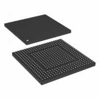
MPC8308VMAGD Freescale Semiconductor, MPC8308VMAGD Datasheet - Page 200

MPC8308VMAGD
Manufacturer Part Number
MPC8308VMAGD
Description
MPU POWERQUICC II PRO 473MAPBGA
Manufacturer
Freescale Semiconductor
Datasheets
1.MPC8308VMAGD.pdf
(90 pages)
2.MPC8308VMAGD.pdf
(2 pages)
3.MPC8308VMAGD.pdf
(1170 pages)
4.MPC8308VMAGD.pdf
(14 pages)
Specifications of MPC8308VMAGD
Processor Type
MPC83xx PowerQUICC II Pro 32-Bit
Speed
400MHz
Voltage
1V
Mounting Type
Surface Mount
Package / Case
473-MAPBGA
Product
Network Processor
Data Rate
256 bps
Frequency
400 MHz
Supply Voltage (max)
3.6 V
Supply Voltage (min)
3 V
Supply Current (max)
5 uA
Maximum Operating Temperature
+ 105 C
Minimum Operating Temperature
0 C
Interface
I2C, JTAG, SPI
Mounting Style
SMD/SMT
Lead Free Status / RoHS Status
Lead free / RoHS Compliant
Features
-
Lead Free Status / Rohs Status
Lead free / RoHS Compliant
Available stocks
Company
Part Number
Manufacturer
Quantity
Price
Company:
Part Number:
MPC8308VMAGD
Manufacturer:
FREESCAL
Quantity:
300
Company:
Part Number:
MPC8308VMAGD
Manufacturer:
Freescale Semiconductor
Quantity:
10 000
Part Number:
MPC8308VMAGD
Manufacturer:
FREESCALE
Quantity:
20 000
Company:
Part Number:
MPC8308VMAGD400/266
Manufacturer:
FREESCAL
Quantity:
300
Company:
Part Number:
MPC8308VMAGDA
Manufacturer:
Freescale Semiconductor
Quantity:
10 000
- MPC8308VMAGD PDF datasheet
- MPC8308VMAGD PDF datasheet #2
- MPC8308VMAGD PDF datasheet #3
- MPC8308VMAGD PDF datasheet #4
- Current page: 200 of 1170
- Download datasheet (9Mb)
System Configuration
5.6.5.1
The global timers configuration registers (GTCFR1 and GTCFR2), shown in
contain configuration parameters used by the timers. These registers allow simultaneous starting, stopping
and resetting of a pair of timers (1 and 2 or 3 and 4) or of a groups of timers (1, 2, 3, and 4) if one bus cycle
is used. GTCFR is cleared by reset.
Table 5-56
5-58
Offset 0x00
Reset
Bits
0
1
Offset
0x03A
0x03C
0x03E
0x038
W
R
Name
PCAS
BCM
PCAS
defines the bit fields of GTCFR1.
0
Global Timers Configuration Registers (GTCFR n )
For proper operation of the timers, do not change the modes of operation and
enable the timer in the same register write operation. The modes can be
changed when GTCFRn[RSTn] is cleared. However, when GTCFRn[RSTn]
are set, they are the only bits that can be changed.
Timer 1 global timers prescale register (GTPSR1)
Timer 2 global timers prescale register (GTPSR2)
Timer 3 global timers prescale register (GTPSR3)
Timer 4 global timers prescale register (GTPSR4)
Pair-cascade mode
0 Normal operation
1 Timers 1 and 2 cascade to form a 32-bit timer.
Note: This bit is ignored in super-cascade mode (GTCFR2[SCAS] = 1).
Note: It is allowed to change the value of this bit only when the corresponding timers are in reset mode.
Backward-compatible mode
0 Provide backward compatibility to PowerQUICC II family timers. In this mode GTCFR1[GM2] bit controls
1 Normal operational mode
the gate mode for timers 1 and 2 and GTCFR2[GM4] bit controls the gate mode for timers 3 and 4.
GTCFR1[GM1] and GTCFR2[GM3] bits are ignored.
Figure 5-43. Global Timers Configuration Register 1 (GTCFR1)
Thus, the user should first clear the RST1 and RST2 bits (without changing PCAS) and then, in a
separate write to the register, change the value of PCAS.
BCM
MPC8308 PowerQUICC II Pro Processor Reference Manual, Rev. 0
1
Table 5-55. GTM Register Address Map (continued)
STP2
Table 5-56. GTCFR1 Bit Settings
2
Register
RST2
3
NOTE
All zeros
Description
GM2
4
GM1
5
Access
Figure 5-43
R/W
STP1
0x0003
Freescale Semiconductor
Reset
Value
6
Access: Read/Write
and
Figure
5.6.5.7/5-64
Section/
RST1
Page
7
5-44,
Related parts for MPC8308VMAGD
Image
Part Number
Description
Manufacturer
Datasheet
Request
R
Part Number:
Description:
Development Boards & Kits - Other Processors MPC8308-NSG
Manufacturer:
Freescale Semiconductor
Datasheet:

Part Number:
Description:
MCU, MPU & DSP Development Tools For MPC8308 Ethernet USB I2C SPI
Manufacturer:
Freescale Semiconductor
Datasheet:

Part Number:
Description:
MCU, MPU & DSP Development Tools For MPC8308 Ethernet USB 32bit
Manufacturer:
Freescale Semiconductor
Datasheet:
Part Number:
Description:
Mpc8308 Powerquicc Ii Pro Processor Hardware Specification
Manufacturer:
Freescale Semiconductor, Inc
Datasheet:

Part Number:
Description:
BOARD REF DESIGN MPC8308
Manufacturer:
Freescale Semiconductor
Datasheet:

Part Number:
Description:
MPC8308 PowerQUICC II Pro Processor Hardware Specification
Manufacturer:
FREESCALE [Freescale Semiconductor, Inc]
Datasheet:
Part Number:
Description:
Microprocessors - MPU E300 ext tmp Qual266
Manufacturer:
Freescale Semiconductor
Datasheet:
Part Number:
Description:
Microprocessors - MPU E300 ext tmp Qual333
Manufacturer:
Freescale Semiconductor
Datasheet:
Part Number:
Description:
Microprocessors - MPU E300 EXT TEMP PB 400
Manufacturer:
Freescale Semiconductor
Datasheet:
Part Number:
Description:
Microprocessors - MPU E300 MP Pb 266
Manufacturer:
Freescale Semiconductor
Datasheet:
Part Number:
Description:
Microprocessors - MPU E300 MP Pb 400
Manufacturer:
Freescale Semiconductor
Datasheet:
Part Number:
Description:
Microprocessors - MPU E300 MP Pb 333
Manufacturer:
Freescale Semiconductor
Datasheet:
Part Number:
Description:
Manufacturer:
Freescale Semiconductor, Inc
Datasheet:
Part Number:
Description:
Manufacturer:
Freescale Semiconductor, Inc
Datasheet:
Part Number:
Description:
Manufacturer:
Freescale Semiconductor, Inc
Datasheet:


