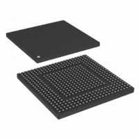
MPC8308VMAGD Freescale Semiconductor, MPC8308VMAGD Datasheet - Page 444

MPC8308VMAGD
Manufacturer Part Number
MPC8308VMAGD
Description
MPU POWERQUICC II PRO 473MAPBGA
Manufacturer
Freescale Semiconductor
Datasheets
1.MPC8308VMAGD.pdf
(90 pages)
2.MPC8308VMAGD.pdf
(2 pages)
3.MPC8308VMAGD.pdf
(1170 pages)
4.MPC8308VMAGD.pdf
(14 pages)
Specifications of MPC8308VMAGD
Processor Type
MPC83xx PowerQUICC II Pro 32-Bit
Speed
400MHz
Voltage
1V
Mounting Type
Surface Mount
Package / Case
473-MAPBGA
Product
Network Processor
Data Rate
256 bps
Frequency
400 MHz
Supply Voltage (max)
3.6 V
Supply Voltage (min)
3 V
Supply Current (max)
5 uA
Maximum Operating Temperature
+ 105 C
Minimum Operating Temperature
0 C
Interface
I2C, JTAG, SPI
Mounting Style
SMD/SMT
Lead Free Status / RoHS Status
Lead free / RoHS Compliant
Features
-
Lead Free Status / Rohs Status
Lead free / RoHS Compliant
Available stocks
Company
Part Number
Manufacturer
Quantity
Price
Company:
Part Number:
MPC8308VMAGD
Manufacturer:
FREESCAL
Quantity:
300
Company:
Part Number:
MPC8308VMAGD
Manufacturer:
Freescale Semiconductor
Quantity:
10 000
Part Number:
MPC8308VMAGD
Manufacturer:
FREESCALE
Quantity:
20 000
Company:
Part Number:
MPC8308VMAGD400/266
Manufacturer:
FREESCAL
Quantity:
300
Company:
Part Number:
MPC8308VMAGDA
Manufacturer:
Freescale Semiconductor
Quantity:
10 000
- MPC8308VMAGD PDF datasheet
- MPC8308VMAGD PDF datasheet #2
- MPC8308VMAGD PDF datasheet #3
- MPC8308VMAGD PDF datasheet #4
- Current page: 444 of 1170
- Download datasheet (9Mb)
Enhanced Local Bus Controller
10.4.3.3.4
The timing for read data transfers is shown in
enable its output drivers and drive valid read data while LFRE is held low. FCM samples read data on the
rising edge of LFRE, which follows an optional number of wait states. Note that FCM will delay the first
read if a RBW or RSW instruction is issued, in which case LFRB sample timing takes effect (see
Section 10.4.3.3.3, “FCM Ready/Busy
10-64
LCLK
(unused)
LFWE0
LFCLE/
LFALE
LFRE
LD[0:7]
TA
LFCLE
LFWE
LFRB
LFRE
write cycle
write data
FCM Read Data Timing
long-latency CW command issue
TRLX = 0:
TRLX = 1:
Notes:
MPC8308 PowerQUICC II Pro Processor Reference Manual, Rev. 0
Figure 10-54. FCM Delay Prior to Sampling LFRB State
t
t
t
RP
RHT
WRT
8×(2+SCY) cycles
16×(2+SCY) LCLK cycles
(for TRLX = 0, RST = 0, SCY = 1, CLKDIV = 4*N)
= LFRE pulse time, read period.
= LFRE hold time.
= Write to read turnaround time.
Figure 10-55. FCM Read Data Timing
Timing”).
write-to-read turnaround
Figure
LFRB sample
t
WRT
points
10-55. Upon assertion of LFRE, the Flash device will
NAND FlashFlash busy state
t
t
WS
RC
= Read data cycle time.
= Read wait state time.
read cycle
t
RP
read data
t
t
WS
ready state
RC
FCM continues
following LFRB high
Freescale Semiconductor
t
RHT
sample data
Related parts for MPC8308VMAGD
Image
Part Number
Description
Manufacturer
Datasheet
Request
R
Part Number:
Description:
Development Boards & Kits - Other Processors MPC8308-NSG
Manufacturer:
Freescale Semiconductor
Datasheet:

Part Number:
Description:
MCU, MPU & DSP Development Tools For MPC8308 Ethernet USB I2C SPI
Manufacturer:
Freescale Semiconductor
Datasheet:

Part Number:
Description:
MCU, MPU & DSP Development Tools For MPC8308 Ethernet USB 32bit
Manufacturer:
Freescale Semiconductor
Datasheet:
Part Number:
Description:
Mpc8308 Powerquicc Ii Pro Processor Hardware Specification
Manufacturer:
Freescale Semiconductor, Inc
Datasheet:

Part Number:
Description:
BOARD REF DESIGN MPC8308
Manufacturer:
Freescale Semiconductor
Datasheet:

Part Number:
Description:
MPC8308 PowerQUICC II Pro Processor Hardware Specification
Manufacturer:
FREESCALE [Freescale Semiconductor, Inc]
Datasheet:
Part Number:
Description:
Microprocessors - MPU E300 ext tmp Qual266
Manufacturer:
Freescale Semiconductor
Datasheet:
Part Number:
Description:
Microprocessors - MPU E300 ext tmp Qual333
Manufacturer:
Freescale Semiconductor
Datasheet:
Part Number:
Description:
Microprocessors - MPU E300 EXT TEMP PB 400
Manufacturer:
Freescale Semiconductor
Datasheet:
Part Number:
Description:
Microprocessors - MPU E300 MP Pb 266
Manufacturer:
Freescale Semiconductor
Datasheet:
Part Number:
Description:
Microprocessors - MPU E300 MP Pb 400
Manufacturer:
Freescale Semiconductor
Datasheet:
Part Number:
Description:
Microprocessors - MPU E300 MP Pb 333
Manufacturer:
Freescale Semiconductor
Datasheet:
Part Number:
Description:
Manufacturer:
Freescale Semiconductor, Inc
Datasheet:
Part Number:
Description:
Manufacturer:
Freescale Semiconductor, Inc
Datasheet:
Part Number:
Description:
Manufacturer:
Freescale Semiconductor, Inc
Datasheet:


