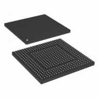
MPC8308VMAGD Freescale Semiconductor, MPC8308VMAGD Datasheet - Page 167

MPC8308VMAGD
Manufacturer Part Number
MPC8308VMAGD
Description
MPU POWERQUICC II PRO 473MAPBGA
Manufacturer
Freescale Semiconductor
Datasheets
1.MPC8308VMAGD.pdf
(90 pages)
2.MPC8308VMAGD.pdf
(2 pages)
3.MPC8308VMAGD.pdf
(1170 pages)
4.MPC8308VMAGD.pdf
(14 pages)
Specifications of MPC8308VMAGD
Processor Type
MPC83xx PowerQUICC II Pro 32-Bit
Speed
400MHz
Voltage
1V
Mounting Type
Surface Mount
Package / Case
473-MAPBGA
Product
Network Processor
Data Rate
256 bps
Frequency
400 MHz
Supply Voltage (max)
3.6 V
Supply Voltage (min)
3 V
Supply Current (max)
5 uA
Maximum Operating Temperature
+ 105 C
Minimum Operating Temperature
0 C
Interface
I2C, JTAG, SPI
Mounting Style
SMD/SMT
Lead Free Status / RoHS Status
Lead free / RoHS Compliant
Features
-
Lead Free Status / Rohs Status
Lead free / RoHS Compliant
Available stocks
Company
Part Number
Manufacturer
Quantity
Price
Company:
Part Number:
MPC8308VMAGD
Manufacturer:
FREESCAL
Quantity:
300
Company:
Part Number:
MPC8308VMAGD
Manufacturer:
Freescale Semiconductor
Quantity:
10 000
Part Number:
MPC8308VMAGD
Manufacturer:
FREESCALE
Quantity:
20 000
Company:
Part Number:
MPC8308VMAGD400/266
Manufacturer:
FREESCAL
Quantity:
300
Company:
Part Number:
MPC8308VMAGDA
Manufacturer:
Freescale Semiconductor
Quantity:
10 000
- MPC8308VMAGD PDF datasheet
- MPC8308VMAGD PDF datasheet #2
- MPC8308VMAGD PDF datasheet #3
- MPC8308VMAGD PDF datasheet #4
- Current page: 167 of 1170
- Download datasheet (9Mb)
1
2
24–26
28–29
1
2
Freescale Semiconductor
Bits
27
30
31
When SICRH[eSDHC_A] = 0b01, SD_CLK and SD_CMD are in High-Z state.
To enable the GPIO functionality, this bit must be programmed to 11.
Bits
If RCWH[ETSEC1M] is RGMII, the reset value is 1; otherwise, it is 0
If RCWH[ETSEC2M] is RGMII, the reset value is 1; otherwise, it is 0.
23
27
30
31
SICRH[Bits] Value
TMROBI
TSOBI1
TSOBI2
Group
GPIO_SEL
TMROBI
TSOBI1
TSOBI2
—
—
Name
An empty column cannot be used for this register. A function should be
selected so that the column is non-empty.
MPC8308 PowerQUICC II Pro Processor Reference Manual, Rev. 0
GPIO[0:15] is provided at two places. This bit selects the position of the
GPIO registers.
0 Primary GPIO[0:15] provided as function-0, selectable through GPIO_A
1 GPIO[0:15] provided in function-3, selectable through GTM,
IEEE1588 timer TSEC_TMR ports output buffer impedance. This bit
controls the output buffer impedance of the TMR output/input signals used
for reduced pin mode interfaces (RGMII). The output buffer impedance
should be correlated to the voltage supplied to the TSEC1 I/O pins (LVDD1).
For non-eTSEC mode of operation, this bit must be cleared.
0 Output buffer is set for 40 Ω, 3.3 V.
1 Output buffer is set for 40 Ω, 2.5 V.
TSEC1 output buffer impedance. This bit controls the output buffer
impedance of the TSEC1 output signals, used for reduced pin mode
interfaces (RGMII). The output buffer impedance should be correlated to the
voltage supplied to the TSEC1 I/O pins (LVDD1). For non-eTSEC mode of
operation, this bit must be cleared.
0 Output buffer is set for 40 Ω, 3.3 V.
1 Output buffer is set for 40 Ω, 2.5 V.
TSEC2 output buffer impedance. This bit controls the output buffer
impedance of TSEC2 output signals, used for reduced pin mode interfaces
(RGMII). The output buffer impedance should be correlated to the voltage
supplied to the TSEC2 I/O pins (LVDD2).
0 Output buffer is set for 40 Ω, 3.3 V.
1 Output buffer is set for 40 Ω, 2.5 V.
Pin Function 0
and GPIO_B.
IEEE1588_A, IEEE1588_B, and ETSEC2.
Reserved
Reserved
Table 5-26. SICRH Bit Settings (continued)
0b00
Table 5-27. SICRH[27–31] Bit Settings
See
See
NOTE
Table 5-27
Table 5-27
Pin Function 1
Description
0b01
—
—
for description and reset value.
for description and reset value.
Pin Function 2
0b10
—
—
Pin Function 3
System Configuration
0b11
—
—
0 Else
1 RGMII
0 Else
1 RGMII
Reset Value
0
0
1
2
Reset
Value
—
—
5-25
Related parts for MPC8308VMAGD
Image
Part Number
Description
Manufacturer
Datasheet
Request
R
Part Number:
Description:
Development Boards & Kits - Other Processors MPC8308-NSG
Manufacturer:
Freescale Semiconductor
Datasheet:

Part Number:
Description:
MCU, MPU & DSP Development Tools For MPC8308 Ethernet USB I2C SPI
Manufacturer:
Freescale Semiconductor
Datasheet:

Part Number:
Description:
MCU, MPU & DSP Development Tools For MPC8308 Ethernet USB 32bit
Manufacturer:
Freescale Semiconductor
Datasheet:
Part Number:
Description:
Mpc8308 Powerquicc Ii Pro Processor Hardware Specification
Manufacturer:
Freescale Semiconductor, Inc
Datasheet:

Part Number:
Description:
BOARD REF DESIGN MPC8308
Manufacturer:
Freescale Semiconductor
Datasheet:

Part Number:
Description:
MPC8308 PowerQUICC II Pro Processor Hardware Specification
Manufacturer:
FREESCALE [Freescale Semiconductor, Inc]
Datasheet:
Part Number:
Description:
Microprocessors - MPU E300 ext tmp Qual266
Manufacturer:
Freescale Semiconductor
Datasheet:
Part Number:
Description:
Microprocessors - MPU E300 ext tmp Qual333
Manufacturer:
Freescale Semiconductor
Datasheet:
Part Number:
Description:
Microprocessors - MPU E300 EXT TEMP PB 400
Manufacturer:
Freescale Semiconductor
Datasheet:
Part Number:
Description:
Microprocessors - MPU E300 MP Pb 266
Manufacturer:
Freescale Semiconductor
Datasheet:
Part Number:
Description:
Microprocessors - MPU E300 MP Pb 400
Manufacturer:
Freescale Semiconductor
Datasheet:
Part Number:
Description:
Microprocessors - MPU E300 MP Pb 333
Manufacturer:
Freescale Semiconductor
Datasheet:
Part Number:
Description:
Manufacturer:
Freescale Semiconductor, Inc
Datasheet:
Part Number:
Description:
Manufacturer:
Freescale Semiconductor, Inc
Datasheet:
Part Number:
Description:
Manufacturer:
Freescale Semiconductor, Inc
Datasheet:


