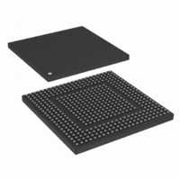
MPC8308VMAGD Freescale Semiconductor, MPC8308VMAGD Datasheet - Page 1132

MPC8308VMAGD
Manufacturer Part Number
MPC8308VMAGD
Description
MPU POWERQUICC II PRO 473MAPBGA
Manufacturer
Freescale Semiconductor
Datasheets
1.MPC8308VMAGD.pdf
(90 pages)
2.MPC8308VMAGD.pdf
(2 pages)
3.MPC8308VMAGD.pdf
(1170 pages)
4.MPC8308VMAGD.pdf
(14 pages)
Specifications of MPC8308VMAGD
Processor Type
MPC83xx PowerQUICC II Pro 32-Bit
Speed
400MHz
Voltage
1V
Mounting Type
Surface Mount
Package / Case
473-MAPBGA
Product
Network Processor
Data Rate
256 bps
Frequency
400 MHz
Supply Voltage (max)
3.6 V
Supply Voltage (min)
3 V
Supply Current (max)
5 uA
Maximum Operating Temperature
+ 105 C
Minimum Operating Temperature
0 C
Interface
I2C, JTAG, SPI
Mounting Style
SMD/SMT
Lead Free Status / RoHS Status
Lead free / RoHS Compliant
Features
-
Lead Free Status / Rohs Status
Lead free / RoHS Compliant
Available stocks
Company
Part Number
Manufacturer
Quantity
Price
Company:
Part Number:
MPC8308VMAGD
Manufacturer:
FREESCAL
Quantity:
300
Company:
Part Number:
MPC8308VMAGD
Manufacturer:
Freescale Semiconductor
Quantity:
10 000
Part Number:
MPC8308VMAGD
Manufacturer:
FREESCALE
Quantity:
20 000
Company:
Part Number:
MPC8308VMAGD400/266
Manufacturer:
FREESCAL
Quantity:
300
Company:
Part Number:
MPC8308VMAGDA
Manufacturer:
Freescale Semiconductor
Quantity:
10 000
- MPC8308VMAGD PDF datasheet
- MPC8308VMAGD PDF datasheet #2
- MPC8308VMAGD PDF datasheet #3
- MPC8308VMAGD PDF datasheet #4
- Current page: 1132 of 1170
- Download datasheet (9Mb)
General Purpose I/O (GPIO)
21.2
The following section provides information about GPIO signals.
21.2.1
Table 21-1
21.3
The GPIO has programmable registers that occupy 24 bytes of memory-mapped space. Note that reading
undefined portions of the memory map returns all zeros and writing has no effect.
All GPIO registers are 32 bits wide and are located on 32-bit address boundaries. All addresses used in this
chapter are offsets from the address held in IMMRBAR as defined in
Table 21-2
21-2
GPIO[0:23]
0xC0C
Offset
0xC00
0xC04
0xC08
0xC10
0xC14
•
•
Signal
Open-drain capability on all ports
All ports can optionally generate an interrupt upon changing their state.
Memory Map/Register Definition
External Signal Description
provides detailed descriptions of the external GPIO signals.
shows the memory map of GPIO.
Signals Overview
GPIO direction register (GPDIR)
GPIO open drain register (GPODR)
GPIO data register (GPDAT)
GPIO interrupt event register (GPIER)
GPIO interrupt mask register (GPIMR)
GPIO external interrupt control register (GPICR)
I/O
I/O General purpose I/O. Each signal can be set individually to act as input or output, according to application
needs.
Meaning
Timing Assertion/Negation—Inputs can be asserted completely asynchronously.
State
MPC8308 PowerQUICC II Pro Processor Reference Manual, Rev. 0
General Purpose I/O (GPIO)—Block Base Address 0x0_0C00
Asserted/Negated—Defined per application.
Outputs are asynchronous to any externally visible clock
Table 21-2. GPIO Register Address Map
Table 21-1. GPIO—Signal Descriptions
Register
Description
Access
R/W
R/W
R/W
R/W
R/W
w1c
Chapter 3, “Memory Map.”
0x0000_0000
0x0000_0000
0x0000_0000
0x0000_0000
0x0000_0000
Reset Value
Undefined
Freescale Semiconductor
Section/Page
21.3.1/21-3
21.3.2/21-3
21.3.3/21-4
21.3.4/21-4
21.3.5/21-4
21.3.6/21-5
Related parts for MPC8308VMAGD
Image
Part Number
Description
Manufacturer
Datasheet
Request
R
Part Number:
Description:
Development Boards & Kits - Other Processors MPC8308-NSG
Manufacturer:
Freescale Semiconductor
Datasheet:

Part Number:
Description:
MCU, MPU & DSP Development Tools For MPC8308 Ethernet USB I2C SPI
Manufacturer:
Freescale Semiconductor
Datasheet:

Part Number:
Description:
MCU, MPU & DSP Development Tools For MPC8308 Ethernet USB 32bit
Manufacturer:
Freescale Semiconductor
Datasheet:
Part Number:
Description:
Mpc8308 Powerquicc Ii Pro Processor Hardware Specification
Manufacturer:
Freescale Semiconductor, Inc
Datasheet:

Part Number:
Description:
BOARD REF DESIGN MPC8308
Manufacturer:
Freescale Semiconductor
Datasheet:

Part Number:
Description:
MPC8308 PowerQUICC II Pro Processor Hardware Specification
Manufacturer:
FREESCALE [Freescale Semiconductor, Inc]
Datasheet:
Part Number:
Description:
Microprocessors - MPU E300 ext tmp Qual266
Manufacturer:
Freescale Semiconductor
Datasheet:
Part Number:
Description:
Microprocessors - MPU E300 ext tmp Qual333
Manufacturer:
Freescale Semiconductor
Datasheet:
Part Number:
Description:
Microprocessors - MPU E300 EXT TEMP PB 400
Manufacturer:
Freescale Semiconductor
Datasheet:
Part Number:
Description:
Microprocessors - MPU E300 MP Pb 266
Manufacturer:
Freescale Semiconductor
Datasheet:
Part Number:
Description:
Microprocessors - MPU E300 MP Pb 400
Manufacturer:
Freescale Semiconductor
Datasheet:
Part Number:
Description:
Microprocessors - MPU E300 MP Pb 333
Manufacturer:
Freescale Semiconductor
Datasheet:
Part Number:
Description:
Manufacturer:
Freescale Semiconductor, Inc
Datasheet:
Part Number:
Description:
Manufacturer:
Freescale Semiconductor, Inc
Datasheet:
Part Number:
Description:
Manufacturer:
Freescale Semiconductor, Inc
Datasheet:


