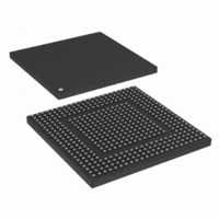
MPC8308VMAGD Freescale Semiconductor, MPC8308VMAGD Datasheet - Page 105

MPC8308VMAGD
Manufacturer Part Number
MPC8308VMAGD
Description
MPU POWERQUICC II PRO 473MAPBGA
Manufacturer
Freescale Semiconductor
Datasheets
1.MPC8308VMAGD.pdf
(90 pages)
2.MPC8308VMAGD.pdf
(2 pages)
3.MPC8308VMAGD.pdf
(1170 pages)
4.MPC8308VMAGD.pdf
(14 pages)
Specifications of MPC8308VMAGD
Processor Type
MPC83xx PowerQUICC II Pro 32-Bit
Speed
400MHz
Voltage
1V
Mounting Type
Surface Mount
Package / Case
473-MAPBGA
Product
Network Processor
Data Rate
256 bps
Frequency
400 MHz
Supply Voltage (max)
3.6 V
Supply Voltage (min)
3 V
Supply Current (max)
5 uA
Maximum Operating Temperature
+ 105 C
Minimum Operating Temperature
0 C
Interface
I2C, JTAG, SPI
Mounting Style
SMD/SMT
Lead Free Status / RoHS Status
Lead free / RoHS Compliant
Features
-
Lead Free Status / Rohs Status
Lead free / RoHS Compliant
Available stocks
Company
Part Number
Manufacturer
Quantity
Price
Company:
Part Number:
MPC8308VMAGD
Manufacturer:
FREESCAL
Quantity:
300
Company:
Part Number:
MPC8308VMAGD
Manufacturer:
Freescale Semiconductor
Quantity:
10 000
Part Number:
MPC8308VMAGD
Manufacturer:
FREESCALE
Quantity:
20 000
Company:
Part Number:
MPC8308VMAGD400/266
Manufacturer:
FREESCAL
Quantity:
300
Company:
Part Number:
MPC8308VMAGDA
Manufacturer:
Freescale Semiconductor
Quantity:
10 000
- MPC8308VMAGD PDF datasheet
- MPC8308VMAGD PDF datasheet #2
- MPC8308VMAGD PDF datasheet #3
- MPC8308VMAGD PDF datasheet #4
- Current page: 105 of 1170
- Download datasheet (9Mb)
Chapter 3
Memory Map
This chapter describes the MPC8308 memory map. The internal memory-mapped registers are described,
including a complete listing of all memory-mapped registers with cross references to the sections detailing
descriptions of each.
3.1
All of the memory-mapped registers in the device are contained within a 1-Mbyte address region. To allow
for flexibility, the base address of the memory-mapped registers is re-locatable in the local address space.
The local address map location of this register block is controlled by the internal memory-mapped registers
base address register (IMMRBAR). See
Register (IMMRBAR),”
3.2
When the local e300 processor is used to configure IMMR space, the IMMR memory space should
typically be marked as cache-inhibited and guarded.
In addition, many configuration registers affect accesses to other memory regions; therefore, writes to
these registers must be guaranteed to have taken effect before accesses are made to the associated memory
regions.
To guarantee that the results of any sequence of writes to configuration registers are in effect, the final
configuration register write should be followed immediately by a read of the same register, and that should
be followed by a sync instruction. Then accesses can safely be made to memory regions affected by the
configuration register write.
3.3
Table 3-1
stated otherwise in a particular block, all accesses to and from the memory-mapped registers must be made
with 32-bit accesses. There is no support for accesses of sizes other than 32 bits.
Reading from address locations that appear as reserved in the memory map table is not guaranteed to return
predictable data. Writing to address locations that appear as reserved in the memory map table is not
allowed and could lead to unpredictable behavior of the device. Reserved bits in non-reserved registers are
read as zero unless the reset value of those bits is different due to internal logic considerations.
When writing to registers with reserved bits, those reserved bits should be cleared. By doing so, existing
software would be able to run on a future modified device in which some reserved bits were allocated for
enhanced modes. This would allow for maintaining the legacy functionality when set to zero.
Freescale Semiconductor
Internal Memory-Mapped Registers
Accessing IMMR Memory from the Local Processor
IMMR Address Map
lists the location of the functional block base addresses for the entire IMMRBAR space. Unless
MPC8308 PowerQUICC II Pro Processor Reference Manual, Rev. 0
for more information. The default value for IMMRBAR is 0xFF40_0000.
Section 5.1.4.1, “Internal Memory Map Registers Base Address
3-1
Related parts for MPC8308VMAGD
Image
Part Number
Description
Manufacturer
Datasheet
Request
R
Part Number:
Description:
Development Boards & Kits - Other Processors MPC8308-NSG
Manufacturer:
Freescale Semiconductor
Datasheet:

Part Number:
Description:
MCU, MPU & DSP Development Tools For MPC8308 Ethernet USB I2C SPI
Manufacturer:
Freescale Semiconductor
Datasheet:

Part Number:
Description:
MCU, MPU & DSP Development Tools For MPC8308 Ethernet USB 32bit
Manufacturer:
Freescale Semiconductor
Datasheet:
Part Number:
Description:
Mpc8308 Powerquicc Ii Pro Processor Hardware Specification
Manufacturer:
Freescale Semiconductor, Inc
Datasheet:

Part Number:
Description:
BOARD REF DESIGN MPC8308
Manufacturer:
Freescale Semiconductor
Datasheet:

Part Number:
Description:
MPC8308 PowerQUICC II Pro Processor Hardware Specification
Manufacturer:
FREESCALE [Freescale Semiconductor, Inc]
Datasheet:
Part Number:
Description:
Microprocessors - MPU E300 ext tmp Qual266
Manufacturer:
Freescale Semiconductor
Datasheet:
Part Number:
Description:
Microprocessors - MPU E300 ext tmp Qual333
Manufacturer:
Freescale Semiconductor
Datasheet:
Part Number:
Description:
Microprocessors - MPU E300 EXT TEMP PB 400
Manufacturer:
Freescale Semiconductor
Datasheet:
Part Number:
Description:
Microprocessors - MPU E300 MP Pb 266
Manufacturer:
Freescale Semiconductor
Datasheet:
Part Number:
Description:
Microprocessors - MPU E300 MP Pb 400
Manufacturer:
Freescale Semiconductor
Datasheet:
Part Number:
Description:
Microprocessors - MPU E300 MP Pb 333
Manufacturer:
Freescale Semiconductor
Datasheet:
Part Number:
Description:
Manufacturer:
Freescale Semiconductor, Inc
Datasheet:
Part Number:
Description:
Manufacturer:
Freescale Semiconductor, Inc
Datasheet:
Part Number:
Description:
Manufacturer:
Freescale Semiconductor, Inc
Datasheet:


