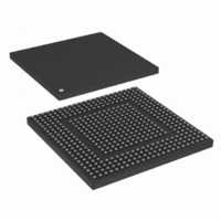
MPC8308VMAGD Freescale Semiconductor, MPC8308VMAGD Datasheet - Page 400

MPC8308VMAGD
Manufacturer Part Number
MPC8308VMAGD
Description
MPU POWERQUICC II PRO 473MAPBGA
Manufacturer
Freescale Semiconductor
Datasheets
1.MPC8308VMAGD.pdf
(90 pages)
2.MPC8308VMAGD.pdf
(2 pages)
3.MPC8308VMAGD.pdf
(1170 pages)
4.MPC8308VMAGD.pdf
(14 pages)
Specifications of MPC8308VMAGD
Processor Type
MPC83xx PowerQUICC II Pro 32-Bit
Speed
400MHz
Voltage
1V
Mounting Type
Surface Mount
Package / Case
473-MAPBGA
Product
Network Processor
Data Rate
256 bps
Frequency
400 MHz
Supply Voltage (max)
3.6 V
Supply Voltage (min)
3 V
Supply Current (max)
5 uA
Maximum Operating Temperature
+ 105 C
Minimum Operating Temperature
0 C
Interface
I2C, JTAG, SPI
Mounting Style
SMD/SMT
Lead Free Status / RoHS Status
Lead free / RoHS Compliant
Features
-
Lead Free Status / Rohs Status
Lead free / RoHS Compliant
Available stocks
Company
Part Number
Manufacturer
Quantity
Price
Company:
Part Number:
MPC8308VMAGD
Manufacturer:
FREESCAL
Quantity:
300
Company:
Part Number:
MPC8308VMAGD
Manufacturer:
Freescale Semiconductor
Quantity:
10 000
Part Number:
MPC8308VMAGD
Manufacturer:
FREESCALE
Quantity:
20 000
Company:
Part Number:
MPC8308VMAGD400/266
Manufacturer:
FREESCAL
Quantity:
300
Company:
Part Number:
MPC8308VMAGDA
Manufacturer:
Freescale Semiconductor
Quantity:
10 000
- MPC8308VMAGD PDF datasheet
- MPC8308VMAGD PDF datasheet #2
- MPC8308VMAGD PDF datasheet #3
- MPC8308VMAGD PDF datasheet #4
- Current page: 400 of 1170
- Download datasheet (9Mb)
Enhanced Local Bus Controller
10-20
10–12
14–17
18–21
Bits
8–9
13
Name
G0CL General line 0 control. Determines which logical address line can be output to the LGPL0 pin when the UPM n
GPL4
WLF
RLF
DS
Disable timer period. Guarantees a minimum time between accesses to the same memory bank controlled
by UPM n . The disable timer is turned on by the TODT bit in the RAM array word, and when expired, the UPM n
allows the machine access to handle a memory pattern to the same bank. Accesses to a different bank by
the same UPM n is also allowed. To avoid conflicts between successive accesses to different banks, the
minimum pattern in the RAM array for a request serviced, should not be shorter than the period established
by DS.
00 1-bus clock cycle disable period
01 2-bus clock cycle disable period
10 3-bus clock cycle disable period
11 4-bus clock cycle disable period
is selected to control the memory access.
000 A12
001 A11
010 A10
011 A9
100 A8
101 A7
110 A6
111 A5
LGPL4 output line disable. Determines how the LGPL4/LUPWAIT pin is controlled by the corresponding bits
in the UPM n array. See
Read loop field. Determines the number of times a loop defined in the UPM n will be executed for a burst- or
single-beat read pattern or when M x MR[OP] = 11 (
0000 16
0001 1
0010 2
0011 3
...
1110 14
1111 15
Write loop field. Determines the number of times a loop defined in the UPM n will be executed for a burst- or
single-beat write pattern.
0000 16
0001 1
0010 2
0011 3
...
1110 14
1111 15
Value
MPC8308 PowerQUICC II Pro Processor Reference Manual, Rev. 0
0
1
Table 10-11. M x MR Field Descriptions (continued)
LGPL4/LUPWAIT
LUPWAIT (input)
LGPL4 (output)
Pin Function
Table 10-40 on page
Interpretation of UPM Word Bits
G4T1/DLT3
10-75.
Description
G4T1
DLT3
RUN
command)
G4T3/WAEN
WAEN
G4T3
Freescale Semiconductor
Related parts for MPC8308VMAGD
Image
Part Number
Description
Manufacturer
Datasheet
Request
R
Part Number:
Description:
Development Boards & Kits - Other Processors MPC8308-NSG
Manufacturer:
Freescale Semiconductor
Datasheet:

Part Number:
Description:
MCU, MPU & DSP Development Tools For MPC8308 Ethernet USB I2C SPI
Manufacturer:
Freescale Semiconductor
Datasheet:

Part Number:
Description:
MCU, MPU & DSP Development Tools For MPC8308 Ethernet USB 32bit
Manufacturer:
Freescale Semiconductor
Datasheet:
Part Number:
Description:
Mpc8308 Powerquicc Ii Pro Processor Hardware Specification
Manufacturer:
Freescale Semiconductor, Inc
Datasheet:

Part Number:
Description:
BOARD REF DESIGN MPC8308
Manufacturer:
Freescale Semiconductor
Datasheet:

Part Number:
Description:
MPC8308 PowerQUICC II Pro Processor Hardware Specification
Manufacturer:
FREESCALE [Freescale Semiconductor, Inc]
Datasheet:
Part Number:
Description:
Microprocessors - MPU E300 ext tmp Qual266
Manufacturer:
Freescale Semiconductor
Datasheet:
Part Number:
Description:
Microprocessors - MPU E300 ext tmp Qual333
Manufacturer:
Freescale Semiconductor
Datasheet:
Part Number:
Description:
Microprocessors - MPU E300 EXT TEMP PB 400
Manufacturer:
Freescale Semiconductor
Datasheet:
Part Number:
Description:
Microprocessors - MPU E300 MP Pb 266
Manufacturer:
Freescale Semiconductor
Datasheet:
Part Number:
Description:
Microprocessors - MPU E300 MP Pb 400
Manufacturer:
Freescale Semiconductor
Datasheet:
Part Number:
Description:
Microprocessors - MPU E300 MP Pb 333
Manufacturer:
Freescale Semiconductor
Datasheet:
Part Number:
Description:
Manufacturer:
Freescale Semiconductor, Inc
Datasheet:
Part Number:
Description:
Manufacturer:
Freescale Semiconductor, Inc
Datasheet:
Part Number:
Description:
Manufacturer:
Freescale Semiconductor, Inc
Datasheet:


