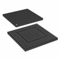
MPC8308VMAGD Freescale Semiconductor, MPC8308VMAGD Datasheet - Page 414

MPC8308VMAGD
Manufacturer Part Number
MPC8308VMAGD
Description
MPU POWERQUICC II PRO 473MAPBGA
Manufacturer
Freescale Semiconductor
Datasheets
1.MPC8308VMAGD.pdf
(90 pages)
2.MPC8308VMAGD.pdf
(2 pages)
3.MPC8308VMAGD.pdf
(1170 pages)
4.MPC8308VMAGD.pdf
(14 pages)
Specifications of MPC8308VMAGD
Processor Type
MPC83xx PowerQUICC II Pro 32-Bit
Speed
400MHz
Voltage
1V
Mounting Type
Surface Mount
Package / Case
473-MAPBGA
Product
Network Processor
Data Rate
256 bps
Frequency
400 MHz
Supply Voltage (max)
3.6 V
Supply Voltage (min)
3 V
Supply Current (max)
5 uA
Maximum Operating Temperature
+ 105 C
Minimum Operating Temperature
0 C
Interface
I2C, JTAG, SPI
Mounting Style
SMD/SMT
Lead Free Status / RoHS Status
Lead free / RoHS Compliant
Features
-
Lead Free Status / Rohs Status
Lead free / RoHS Compliant
Available stocks
Company
Part Number
Manufacturer
Quantity
Price
Company:
Part Number:
MPC8308VMAGD
Manufacturer:
FREESCAL
Quantity:
300
Company:
Part Number:
MPC8308VMAGD
Manufacturer:
Freescale Semiconductor
Quantity:
10 000
Part Number:
MPC8308VMAGD
Manufacturer:
FREESCALE
Quantity:
20 000
Company:
Part Number:
MPC8308VMAGD400/266
Manufacturer:
FREESCAL
Quantity:
300
Company:
Part Number:
MPC8308VMAGDA
Manufacturer:
Freescale Semiconductor
Quantity:
10 000
- MPC8308VMAGD PDF datasheet
- MPC8308VMAGD PDF datasheet #2
- MPC8308VMAGD PDF datasheet #3
- MPC8308VMAGD PDF datasheet #4
- Current page: 414 of 1170
- Download datasheet (9Mb)
Enhanced Local Bus Controller
10.3.1.18 Flash Instruction Register (FIR)
The local bus Flash instruction register (FIR), shown in
instructions for issue by the FCM. Setting FMR[OP] non-zero and writing LSOR or accessing a bank
controlled by FCM causes FCM to read FIR 4 bits at a time, starting at bit 0 and continuing with adjacent
4-bit opcodes, until only NOP opcodes remain. The programmed instruction sequence of OP0, OP1,...,
OP7 is performed on the activated bank, using the data buffer addressed by FPAR. If LTEIR[CCI] = 1 and
LTEDR[CCD] = 0, eLBC will generate an interrupt once the entire sequence has completed, and software
should examine LTEATR and clear its V bit.
10-34
Offset 0x0_50E4
Reset
Software must not alter the contents of the addressed FCM buffer, FIR, MDR, FCR, FBAR, FPAR, or
FBCR while an operation is in progress—or eLBC will behave unpredictably—but software can freely
modify the contents of any currently unused FCM RAM buffer in preparation for the next operation.
26–27
28–29
30–31
Bits
W
R
0
Name
OP0
OP
AL
—
3
Address length. AL sets the number of address bytes issued during page address (PA) operations.
However, the number of address bytes issued for column address (CA) operations is determined by
the device page size (for OR n [PGS] = 0, 1 CA byte is issued; for OR n [PGS] = 1, 2 CA bytes are issued).
00 2 bytes are issued for page addresses, thus a total of 3 (OR n [PGS] = 0) or 4 (OR n [PGS] = 1)
01 3 bytes are issued for page addresses, thus a total of 4 (OR n [PGS] = 0) or 5 (OR n [PGS] = 1)
10 4 bytes are issued for page addresses, thus a total of 5 (OR n [PGS] = 0) or 6 (OR n [PGS] = 1)
11 —
Reserved
Flash operation. For OP not equal to 00, a special operation is triggered on the next write to LSOR or
dummy access to a bank controlled by FCM. Once a special operation has commenced, OP is
automatically reset to 00 by FCM. Individual blocks may be temporarily unlocked for erase and
reprogramming operations.
00 Normal operation. All read and write accesses to banks controlled by FCM access the shared FCM
01 Simulate auto-boot block loading, and set FMR[BOOT]. Boot block loading occurs from the bank
10 Execute the command sequence contained in FIR, but with write protection enabled (pin LFWP
11 Execute the command sequence contained in FIR, but permit the single block identified by
4
address bytes are issued for a {CA,PA} sequence
address bytes are issued for a {CA,PA} sequence
address bytes are issued for a {CA,PA} sequence
buffer RAM. No bus activity is caused by this operation.
triggered on the special operation, therefore the appropriate bank configuration must be initialized
prior to issuing this operation.
asserted low) so that all Flash blocks are protected from accidental erasure and reprogramming.
FBAR[BLK] to be erased or reprogrammed, with pin LFWP remaining high during the access.
OP1
MPC8308 PowerQUICC II Pro Processor Reference Manual, Rev. 0
Table 10-24. FMR Field Descriptions (continued)
7
8
Figure 10-22. Flash Instruction Register
OP2
11 12
OP3
All zeros
15 16
Description
Figure
OP4
10-22, holds a sequence of up to eight
19 20
OP5
23 24
Freescale Semiconductor
OP6
Access: Read/Write
27 28
OP7
31
Related parts for MPC8308VMAGD
Image
Part Number
Description
Manufacturer
Datasheet
Request
R
Part Number:
Description:
Development Boards & Kits - Other Processors MPC8308-NSG
Manufacturer:
Freescale Semiconductor
Datasheet:

Part Number:
Description:
MCU, MPU & DSP Development Tools For MPC8308 Ethernet USB I2C SPI
Manufacturer:
Freescale Semiconductor
Datasheet:

Part Number:
Description:
MCU, MPU & DSP Development Tools For MPC8308 Ethernet USB 32bit
Manufacturer:
Freescale Semiconductor
Datasheet:
Part Number:
Description:
Mpc8308 Powerquicc Ii Pro Processor Hardware Specification
Manufacturer:
Freescale Semiconductor, Inc
Datasheet:

Part Number:
Description:
BOARD REF DESIGN MPC8308
Manufacturer:
Freescale Semiconductor
Datasheet:

Part Number:
Description:
MPC8308 PowerQUICC II Pro Processor Hardware Specification
Manufacturer:
FREESCALE [Freescale Semiconductor, Inc]
Datasheet:
Part Number:
Description:
Microprocessors - MPU E300 ext tmp Qual266
Manufacturer:
Freescale Semiconductor
Datasheet:
Part Number:
Description:
Microprocessors - MPU E300 ext tmp Qual333
Manufacturer:
Freescale Semiconductor
Datasheet:
Part Number:
Description:
Microprocessors - MPU E300 EXT TEMP PB 400
Manufacturer:
Freescale Semiconductor
Datasheet:
Part Number:
Description:
Microprocessors - MPU E300 MP Pb 266
Manufacturer:
Freescale Semiconductor
Datasheet:
Part Number:
Description:
Microprocessors - MPU E300 MP Pb 400
Manufacturer:
Freescale Semiconductor
Datasheet:
Part Number:
Description:
Microprocessors - MPU E300 MP Pb 333
Manufacturer:
Freescale Semiconductor
Datasheet:
Part Number:
Description:
Manufacturer:
Freescale Semiconductor, Inc
Datasheet:
Part Number:
Description:
Manufacturer:
Freescale Semiconductor, Inc
Datasheet:
Part Number:
Description:
Manufacturer:
Freescale Semiconductor, Inc
Datasheet:


