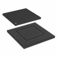
MPC8308VMAGD Freescale Semiconductor, MPC8308VMAGD Datasheet - Page 1082

MPC8308VMAGD
Manufacturer Part Number
MPC8308VMAGD
Description
MPU POWERQUICC II PRO 473MAPBGA
Manufacturer
Freescale Semiconductor
Datasheets
1.MPC8308VMAGD.pdf
(90 pages)
2.MPC8308VMAGD.pdf
(2 pages)
3.MPC8308VMAGD.pdf
(1170 pages)
4.MPC8308VMAGD.pdf
(14 pages)
Specifications of MPC8308VMAGD
Processor Type
MPC83xx PowerQUICC II Pro 32-Bit
Speed
400MHz
Voltage
1V
Mounting Type
Surface Mount
Package / Case
473-MAPBGA
Product
Network Processor
Data Rate
256 bps
Frequency
400 MHz
Supply Voltage (max)
3.6 V
Supply Voltage (min)
3 V
Supply Current (max)
5 uA
Maximum Operating Temperature
+ 105 C
Minimum Operating Temperature
0 C
Interface
I2C, JTAG, SPI
Mounting Style
SMD/SMT
Lead Free Status / RoHS Status
Lead free / RoHS Compliant
Features
-
Lead Free Status / Rohs Status
Lead free / RoHS Compliant
Available stocks
Company
Part Number
Manufacturer
Quantity
Price
Company:
Part Number:
MPC8308VMAGD
Manufacturer:
FREESCAL
Quantity:
300
Company:
Part Number:
MPC8308VMAGD
Manufacturer:
Freescale Semiconductor
Quantity:
10 000
Part Number:
MPC8308VMAGD
Manufacturer:
FREESCALE
Quantity:
20 000
Company:
Part Number:
MPC8308VMAGD400/266
Manufacturer:
FREESCAL
Quantity:
300
Company:
Part Number:
MPC8308VMAGDA
Manufacturer:
Freescale Semiconductor
Quantity:
10 000
- MPC8308VMAGD PDF datasheet
- MPC8308VMAGD PDF datasheet #2
- MPC8308VMAGD PDF datasheet #3
- MPC8308VMAGD PDF datasheet #4
- Current page: 1082 of 1170
- Download datasheet (9Mb)
I
Byte enables should be asserted for any byte that will be written, and they should be asserted contiguously,
creating a 1, 2, or 4 byte write to a register. The boot sequencer assumes that a big-endian address is stored
in the EEPROM. In addition, byte enable bit 0 (bit 1 of the byte) corresponds to the most-significant byte
of data (data[0–7]), and byte enable bit 3 (bit 4 of the byte) corresponds to the least-significant byte of data
(data[24–31]).
By asserting ACS, an alternate configuration space address is prepended to the write request from the boot
sequencer according to the value in the ALTCBAR register. This will allow for external memories to be
configured. Otherwise, IMMRBAR is prepended to the EEPROM address.
If the CONT bit is cleared, the first 3 bytes, including ACS, the byte enables, and the address, should be
cleared 0. Also, the data contains the final CRC. A CRC-32 algorithm is used to check the integrity of the
data. The following polynomial is used:
The CRC should cover all bytes stored in the EEPROM before the CRC. This includes the preamble, all
register preloads, and the first 3 bytes of the last 7-byte preload (which should be all zeros).
17.4.5.4
Dedicated hardware is not provided to indicate whether the boot sequencer operation completed
successfully. It is recommended that one of the GPIO signals be used for that purpose. To do this, the last
register preload programmed into the EEPROM should contain the address of the appropriate GPIO
17-20
2
C Interface
— The first byte holds alternate configuration space (ACS), byte enables, and continue (CONT)
— The 2 least-significant bits of the address are derived from
— The most significant 16 bits (assuming 36-bit addressing) of the address are prepended from
— After the first 3 bytes, 4 bytes of data should hold the desired value of the configuration register,
attributes.
BYTE_ENABLES[ADDRESS_OFFSET]. Therefore, the address offset programmed into the
EEPROM preload should be a word offset.
either IMMRRBAR or alternate configuration space.
regardless of the size of transaction.
1 + x
Boot Sequencer Done Indication
1
Figure 17-10. EEPROM Data Format for One Register Preload Command
+ x
2
+ x
MPC8308 PowerQUICC II Pro Processor Reference Manual, Rev. 0
ACS
0
4
+ x
5
+ x
1
7
+ x
BYTE_EN
2
8
+ x
10
ADDR[14:21]
ADDR[12:29]
DATA[16:23]
DATA[24:31]
DATA[8:15]
3
DATA[0:7]
+ x
11
+ x
4
12
+ x
CONT
5
16
+ x
ADDR[12:13]
22
6
+ x
23
+ x
7
26
+ x
Freescale Semiconductor
32
Related parts for MPC8308VMAGD
Image
Part Number
Description
Manufacturer
Datasheet
Request
R
Part Number:
Description:
Development Boards & Kits - Other Processors MPC8308-NSG
Manufacturer:
Freescale Semiconductor
Datasheet:

Part Number:
Description:
MCU, MPU & DSP Development Tools For MPC8308 Ethernet USB I2C SPI
Manufacturer:
Freescale Semiconductor
Datasheet:

Part Number:
Description:
MCU, MPU & DSP Development Tools For MPC8308 Ethernet USB 32bit
Manufacturer:
Freescale Semiconductor
Datasheet:
Part Number:
Description:
Mpc8308 Powerquicc Ii Pro Processor Hardware Specification
Manufacturer:
Freescale Semiconductor, Inc
Datasheet:

Part Number:
Description:
BOARD REF DESIGN MPC8308
Manufacturer:
Freescale Semiconductor
Datasheet:

Part Number:
Description:
MPC8308 PowerQUICC II Pro Processor Hardware Specification
Manufacturer:
FREESCALE [Freescale Semiconductor, Inc]
Datasheet:
Part Number:
Description:
Microprocessors - MPU E300 ext tmp Qual266
Manufacturer:
Freescale Semiconductor
Datasheet:
Part Number:
Description:
Microprocessors - MPU E300 ext tmp Qual333
Manufacturer:
Freescale Semiconductor
Datasheet:
Part Number:
Description:
Microprocessors - MPU E300 EXT TEMP PB 400
Manufacturer:
Freescale Semiconductor
Datasheet:
Part Number:
Description:
Microprocessors - MPU E300 MP Pb 266
Manufacturer:
Freescale Semiconductor
Datasheet:
Part Number:
Description:
Microprocessors - MPU E300 MP Pb 400
Manufacturer:
Freescale Semiconductor
Datasheet:
Part Number:
Description:
Microprocessors - MPU E300 MP Pb 333
Manufacturer:
Freescale Semiconductor
Datasheet:
Part Number:
Description:
Manufacturer:
Freescale Semiconductor, Inc
Datasheet:
Part Number:
Description:
Manufacturer:
Freescale Semiconductor, Inc
Datasheet:
Part Number:
Description:
Manufacturer:
Freescale Semiconductor, Inc
Datasheet:


