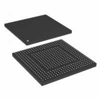
MPC8308VMAGD Freescale Semiconductor, MPC8308VMAGD Datasheet - Page 325

MPC8308VMAGD
Manufacturer Part Number
MPC8308VMAGD
Description
MPU POWERQUICC II PRO 473MAPBGA
Manufacturer
Freescale Semiconductor
Datasheets
1.MPC8308VMAGD.pdf
(90 pages)
2.MPC8308VMAGD.pdf
(2 pages)
3.MPC8308VMAGD.pdf
(1170 pages)
4.MPC8308VMAGD.pdf
(14 pages)
Specifications of MPC8308VMAGD
Processor Type
MPC83xx PowerQUICC II Pro 32-Bit
Speed
400MHz
Voltage
1V
Mounting Type
Surface Mount
Package / Case
473-MAPBGA
Product
Network Processor
Data Rate
256 bps
Frequency
400 MHz
Supply Voltage (max)
3.6 V
Supply Voltage (min)
3 V
Supply Current (max)
5 uA
Maximum Operating Temperature
+ 105 C
Minimum Operating Temperature
0 C
Interface
I2C, JTAG, SPI
Mounting Style
SMD/SMT
Lead Free Status / RoHS Status
Lead free / RoHS Compliant
Features
-
Lead Free Status / Rohs Status
Lead free / RoHS Compliant
Available stocks
Company
Part Number
Manufacturer
Quantity
Price
Company:
Part Number:
MPC8308VMAGD
Manufacturer:
FREESCAL
Quantity:
300
Company:
Part Number:
MPC8308VMAGD
Manufacturer:
Freescale Semiconductor
Quantity:
10 000
Part Number:
MPC8308VMAGD
Manufacturer:
FREESCALE
Quantity:
20 000
Company:
Part Number:
MPC8308VMAGD400/266
Manufacturer:
FREESCAL
Quantity:
300
Company:
Part Number:
MPC8308VMAGDA
Manufacturer:
Freescale Semiconductor
Quantity:
10 000
- MPC8308VMAGD PDF datasheet
- MPC8308VMAGD PDF datasheet #2
- MPC8308VMAGD PDF datasheet #3
- MPC8308VMAGD PDF datasheet #4
- Current page: 325 of 1170
- Download datasheet (9Mb)
Freescale Semiconductor
MECC[0:7]
MBA[2:0]
MA[13:0]
Signal
MCAS
Table 9-3. Memory Interface Signals—Detailed Signal Descriptions (continued)
I/O
I/O Error checking and correcting codes. Input and output signals for the DDR controller’s bidirectional ECC
O
O
O
O
I
bus. MECC[0:5] function in both normal and debug modes.
ECC signals represent the state of ECC driven by the DDR controller on writes. See
“Error Checking and Correcting
As inputs, the ECC signals represent the state of ECC driven by the SDRAM devices on reads.
Address bus. Memory controller outputs for the address to the DRAM. MA[13:0] carry 14 of the address
bits for the DDR memory interface corresponding to the row and column address bits. MA0 is the lsb of
the address output from the memory controller.
SDRAM supports four or eight addressable logical sub-banks. Bit zero of the memory controller’s output
bank address must be connected to bit zero of the SDRAM’s input bank address. MBA0, the
least-significant bit of the three bank address signals, is asserted during the mode register set command
to specify the extended mode register.
Column address strobe. Active-low SDRAM address multiplexing signal. MCAS is asserted for read or
write transactions and for mode register set, refresh, and precharge commands.
Logical bank address. Outputs that drive the logical (or internal) bank address pins of the SDRAM. Each
Meaning
Meaning
Meaning
Meaning
Meaning
Timing Assertion/Negation—Same timing as MDQ
Timing Assertion/Negation—Same timing as MDQ
Timing Assertion/Negation—The address is always driven when the memory controller is enabled.
Timing Assertion/Negation—Same timing as MA n
Timing Assertion/Negation—Assertion and negation timing is directed by the values described in
State
State
State
State
State
MPC8308 PowerQUICC II Pro Processor Reference Manual, Rev. 0
Asserted/Negated—Represents the state of ECC being driven by the DDR controller on
High impedance—Same timing as MDQ
Asserted/Negated—Represents the state of ECC being driven by the DDR SDRAMs on
High impedance—Same timing as MDQ
Asserted/Negated—Represents the address driven by the DDR memory controller. Contains
High impedance—When the memory controller is disabled
Asserted/Negated—Selects the DDR SDRAM logical (or internal) bank to be activated during
High impedance—Same timing as MA n
Asserted—Indicates that a valid SDRAM column address is on the address bus for read and
Negated—The column address is not guaranteed to be valid.
High impedance—MCAS is always driven unless the memory controller is disabled.
writes.
reads.
different portions of the address depending on the memory size and the DRAM
command being issued by the memory controller. See
description of the mapping of these signals.
It is valid when a transaction is driven to DRAM (when MCS n is active).
the row address phase and selects the SDRAM internal bank for the read or write
operation during the column address phase of the memory access.
describes the mapping of these signals in all cases.
write transactions. See
for various other SDRAM commands.
Section 9.4.1.4, “DDR SDRAM Timing Configuration 0 (TIMING_CFG_0),”
Section 9.4.1.5, “DDR SDRAM Timing Configuration 1 (TIMING_CFG_1),”
Section 9.4.1.6, “DDR SDRAM Timing Configuration 2
Section 9.4.1.3, “DDR SDRAM Timing Configuration 3 (TIMING_CFG_3).”
(ECC),” for more details.
Table 9-41
Description
for more information on the states required on MCAS
Table 9-38
(TIMING_CFG_2),” and
DDR Memory Controller
for a complete
Table 9-38
Section 9.5.11,
9-7
Related parts for MPC8308VMAGD
Image
Part Number
Description
Manufacturer
Datasheet
Request
R
Part Number:
Description:
Development Boards & Kits - Other Processors MPC8308-NSG
Manufacturer:
Freescale Semiconductor
Datasheet:

Part Number:
Description:
MCU, MPU & DSP Development Tools For MPC8308 Ethernet USB I2C SPI
Manufacturer:
Freescale Semiconductor
Datasheet:

Part Number:
Description:
MCU, MPU & DSP Development Tools For MPC8308 Ethernet USB 32bit
Manufacturer:
Freescale Semiconductor
Datasheet:
Part Number:
Description:
Mpc8308 Powerquicc Ii Pro Processor Hardware Specification
Manufacturer:
Freescale Semiconductor, Inc
Datasheet:

Part Number:
Description:
BOARD REF DESIGN MPC8308
Manufacturer:
Freescale Semiconductor
Datasheet:

Part Number:
Description:
MPC8308 PowerQUICC II Pro Processor Hardware Specification
Manufacturer:
FREESCALE [Freescale Semiconductor, Inc]
Datasheet:
Part Number:
Description:
Microprocessors - MPU E300 ext tmp Qual266
Manufacturer:
Freescale Semiconductor
Datasheet:
Part Number:
Description:
Microprocessors - MPU E300 ext tmp Qual333
Manufacturer:
Freescale Semiconductor
Datasheet:
Part Number:
Description:
Microprocessors - MPU E300 EXT TEMP PB 400
Manufacturer:
Freescale Semiconductor
Datasheet:
Part Number:
Description:
Microprocessors - MPU E300 MP Pb 266
Manufacturer:
Freescale Semiconductor
Datasheet:
Part Number:
Description:
Microprocessors - MPU E300 MP Pb 400
Manufacturer:
Freescale Semiconductor
Datasheet:
Part Number:
Description:
Microprocessors - MPU E300 MP Pb 333
Manufacturer:
Freescale Semiconductor
Datasheet:
Part Number:
Description:
Manufacturer:
Freescale Semiconductor, Inc
Datasheet:
Part Number:
Description:
Manufacturer:
Freescale Semiconductor, Inc
Datasheet:
Part Number:
Description:
Manufacturer:
Freescale Semiconductor, Inc
Datasheet:


