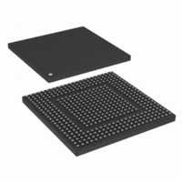
MPC8308VMAGD Freescale Semiconductor, MPC8308VMAGD Datasheet - Page 395

MPC8308VMAGD
Manufacturer Part Number
MPC8308VMAGD
Description
MPU POWERQUICC II PRO 473MAPBGA
Manufacturer
Freescale Semiconductor
Datasheets
1.MPC8308VMAGD.pdf
(90 pages)
2.MPC8308VMAGD.pdf
(2 pages)
3.MPC8308VMAGD.pdf
(1170 pages)
4.MPC8308VMAGD.pdf
(14 pages)
Specifications of MPC8308VMAGD
Processor Type
MPC83xx PowerQUICC II Pro 32-Bit
Speed
400MHz
Voltage
1V
Mounting Type
Surface Mount
Package / Case
473-MAPBGA
Product
Network Processor
Data Rate
256 bps
Frequency
400 MHz
Supply Voltage (max)
3.6 V
Supply Voltage (min)
3 V
Supply Current (max)
5 uA
Maximum Operating Temperature
+ 105 C
Minimum Operating Temperature
0 C
Interface
I2C, JTAG, SPI
Mounting Style
SMD/SMT
Lead Free Status / RoHS Status
Lead free / RoHS Compliant
Features
-
Lead Free Status / Rohs Status
Lead free / RoHS Compliant
Available stocks
Company
Part Number
Manufacturer
Quantity
Price
Company:
Part Number:
MPC8308VMAGD
Manufacturer:
FREESCAL
Quantity:
300
Company:
Part Number:
MPC8308VMAGD
Manufacturer:
Freescale Semiconductor
Quantity:
10 000
Part Number:
MPC8308VMAGD
Manufacturer:
FREESCALE
Quantity:
20 000
Company:
Part Number:
MPC8308VMAGD400/266
Manufacturer:
FREESCAL
Quantity:
300
Company:
Part Number:
MPC8308VMAGDA
Manufacturer:
Freescale Semiconductor
Quantity:
10 000
- MPC8308VMAGD PDF datasheet
- MPC8308VMAGD PDF datasheet #2
- MPC8308VMAGD PDF datasheet #3
- MPC8308VMAGD PDF datasheet #4
- Current page: 395 of 1170
- Download datasheet (9Mb)
Freescale Semiconductor
Bits
19
20
21
22
23
24
BCTLD
Name
CSCT
PGS
CHT
CST
—
Buffer control disable. Disables assertion of LBCTL during access to the current memory bank.
0 LBCTL is asserted upon access to the current memory bank.
1 LBCTL is not asserted upon access to the current memory bank.
Reserved
NAND Flash EEPROM page size, buffer size, and block size.
0 Page size of 512 main area bytes plus 16 spare area bytes (small page devices);
1 Page size of 2048 main area bytes plus 64 spare area bytes (large page devices);
Chip select to command time. Determines how far in advance LCS n is asserted prior to any bus activity
during a NAND Flash access handled by the FCM. This helps meet chip-select setup times for slow
memories.
Command setup time. Determines the delay of LFWE0 assertion relative to the command, address, or data
change when the external memory access is handled by the FCM.
Command hold time. Determines the LFWE0 negation prior to the command, address, or data change
when the external memory access is handled by the FCM.
FCM RAM buffers are 1 Kbyte each; Flash block size of 16 Kbytes.
FCM RAM buffers are 4 Kbytes each; Flash block size of 128 Kbytes.
TRLX
TRLX
TRLX
0
0
1
1
0
0
1
1
0
0
1
1
MPC8308 PowerQUICC II Pro Processor Reference Manual, Rev. 0
Table 10-8. OR n
CSCT
CST
CHT
0
1
0
1
0
1
0
1
0
1
0
1
The chip-select is asserted 1 clock cycle before any command.
The chip-select is asserted 4 clock cycles before any command.
The chip-select is asserted 2 clock cycles before any command.
The chip-select is asserted 8 clock cycles before any command.
The write-enable is asserted coincident with any command.
The write-enable is asserted 0.25 clock cycles after any command, address, or
data.
The write-enable is asserted 0.5 clock cycles after any command, address, or
data.
The write-enable is asserted 1 clock cycle after any command, address, or data.
The write-enable is negated 0.5 clock cycles before any command, address, or
data change.
The write-enable is negated 1 clock cycle before any command, address, or data
change.
The write-enable is negated 1.5 clock cycles before any command, address, or
data change.
The write-enable is negated 2 clock cycles before any command, address, or data
change.
—
FCM Field Descriptions (continued)
Description
Meaning
Meaning
Meaning
Enhanced Local Bus Controller
10-15
Related parts for MPC8308VMAGD
Image
Part Number
Description
Manufacturer
Datasheet
Request
R
Part Number:
Description:
Development Boards & Kits - Other Processors MPC8308-NSG
Manufacturer:
Freescale Semiconductor
Datasheet:

Part Number:
Description:
MCU, MPU & DSP Development Tools For MPC8308 Ethernet USB I2C SPI
Manufacturer:
Freescale Semiconductor
Datasheet:

Part Number:
Description:
MCU, MPU & DSP Development Tools For MPC8308 Ethernet USB 32bit
Manufacturer:
Freescale Semiconductor
Datasheet:
Part Number:
Description:
Mpc8308 Powerquicc Ii Pro Processor Hardware Specification
Manufacturer:
Freescale Semiconductor, Inc
Datasheet:

Part Number:
Description:
BOARD REF DESIGN MPC8308
Manufacturer:
Freescale Semiconductor
Datasheet:

Part Number:
Description:
MPC8308 PowerQUICC II Pro Processor Hardware Specification
Manufacturer:
FREESCALE [Freescale Semiconductor, Inc]
Datasheet:
Part Number:
Description:
Microprocessors - MPU E300 ext tmp Qual266
Manufacturer:
Freescale Semiconductor
Datasheet:
Part Number:
Description:
Microprocessors - MPU E300 ext tmp Qual333
Manufacturer:
Freescale Semiconductor
Datasheet:
Part Number:
Description:
Microprocessors - MPU E300 EXT TEMP PB 400
Manufacturer:
Freescale Semiconductor
Datasheet:
Part Number:
Description:
Microprocessors - MPU E300 MP Pb 266
Manufacturer:
Freescale Semiconductor
Datasheet:
Part Number:
Description:
Microprocessors - MPU E300 MP Pb 400
Manufacturer:
Freescale Semiconductor
Datasheet:
Part Number:
Description:
Microprocessors - MPU E300 MP Pb 333
Manufacturer:
Freescale Semiconductor
Datasheet:
Part Number:
Description:
Manufacturer:
Freescale Semiconductor, Inc
Datasheet:
Part Number:
Description:
Manufacturer:
Freescale Semiconductor, Inc
Datasheet:
Part Number:
Description:
Manufacturer:
Freescale Semiconductor, Inc
Datasheet:


