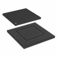
MPC8308VMAGD Freescale Semiconductor, MPC8308VMAGD Datasheet - Page 397

MPC8308VMAGD
Manufacturer Part Number
MPC8308VMAGD
Description
MPU POWERQUICC II PRO 473MAPBGA
Manufacturer
Freescale Semiconductor
Datasheets
1.MPC8308VMAGD.pdf
(90 pages)
2.MPC8308VMAGD.pdf
(2 pages)
3.MPC8308VMAGD.pdf
(1170 pages)
4.MPC8308VMAGD.pdf
(14 pages)
Specifications of MPC8308VMAGD
Processor Type
MPC83xx PowerQUICC II Pro 32-Bit
Speed
400MHz
Voltage
1V
Mounting Type
Surface Mount
Package / Case
473-MAPBGA
Product
Network Processor
Data Rate
256 bps
Frequency
400 MHz
Supply Voltage (max)
3.6 V
Supply Voltage (min)
3 V
Supply Current (max)
5 uA
Maximum Operating Temperature
+ 105 C
Minimum Operating Temperature
0 C
Interface
I2C, JTAG, SPI
Mounting Style
SMD/SMT
Lead Free Status / RoHS Status
Lead free / RoHS Compliant
Features
-
Lead Free Status / Rohs Status
Lead free / RoHS Compliant
Available stocks
Company
Part Number
Manufacturer
Quantity
Price
Company:
Part Number:
MPC8308VMAGD
Manufacturer:
FREESCAL
Quantity:
300
Company:
Part Number:
MPC8308VMAGD
Manufacturer:
Freescale Semiconductor
Quantity:
10 000
Part Number:
MPC8308VMAGD
Manufacturer:
FREESCALE
Quantity:
20 000
Company:
Part Number:
MPC8308VMAGD400/266
Manufacturer:
FREESCAL
Quantity:
300
Company:
Part Number:
MPC8308VMAGDA
Manufacturer:
Freescale Semiconductor
Quantity:
10 000
- MPC8308VMAGD PDF datasheet
- MPC8308VMAGD PDF datasheet #2
- MPC8308VMAGD PDF datasheet #3
- MPC8308VMAGD PDF datasheet #4
- Current page: 397 of 1170
- Download datasheet (9Mb)
1
10.3.1.2.4
Figure 10-5
Table 10-9
Freescale Semiconductor
Offset OR0: 0x0_5004
Reset
Reset
17–18
20–22
24–28
0–16
Bits
Refer to
19
23
29
W
W
R
R
OR1: 0x0_500c
OR2: 0x0_5014
OR3: 0x0_501c
AM
16
BCTLD Buffer control disable. Disables assertion of LBCTL during access to the current memory bank.
0
Name
TRLX
Table 10-5
AM
—
—
BI
—
describes BRn fields for UPM mode.
shows the bit fields for ORn when the corresponding BRn[MSEL] selects a UPM machine.
17
Option Registers (OR n )—UPM Mode
UPM address mask. Masks corresponding BR n bits. Masking address bits independently allows external
devices of different size address ranges to be used. Address mask bits can be set or cleared in any order in
the field, allowing a resource to reside in more than one area of the address map.
0 Corresponding address bits are masked.
1 The corresponding address bits are used in the comparison with address pins.
Reserved
0 LBCTL is asserted upon access to the current memory bank.
1 LBCTL is not asserted upon access to the current memory bank.
Reserved
Burst inhibit. Indicates if this memory bank supports burst accesses.
0 The bank supports burst accesses.
1 The bank does not support burst accesses. The selected UPM executes burst accesses as a series of
Reserved
Timing relaxed. Works in conjunction with EHTR to extend hold time on read accesses.
—
single accesses.
for the OR0 reset value. All other option registers have all bits cleared.
18
MPC8308 PowerQUICC II Pro Processor Reference Manual, Rev. 0
BCTLD
19
Figure 10-5. Option Registers (OR n ) in UPM Mode
Table 10-9. OR n
20
—
22
—
UPM Field Descriptions
23
BI
All zeros
All zeros
AM
Description
24
—
28
Enhanced Local Bus Controller
TRLX
29
Access: Read/Write
EHTR
30
10-17
—
15
31
Related parts for MPC8308VMAGD
Image
Part Number
Description
Manufacturer
Datasheet
Request
R
Part Number:
Description:
Development Boards & Kits - Other Processors MPC8308-NSG
Manufacturer:
Freescale Semiconductor
Datasheet:

Part Number:
Description:
MCU, MPU & DSP Development Tools For MPC8308 Ethernet USB I2C SPI
Manufacturer:
Freescale Semiconductor
Datasheet:

Part Number:
Description:
MCU, MPU & DSP Development Tools For MPC8308 Ethernet USB 32bit
Manufacturer:
Freescale Semiconductor
Datasheet:
Part Number:
Description:
Mpc8308 Powerquicc Ii Pro Processor Hardware Specification
Manufacturer:
Freescale Semiconductor, Inc
Datasheet:

Part Number:
Description:
BOARD REF DESIGN MPC8308
Manufacturer:
Freescale Semiconductor
Datasheet:

Part Number:
Description:
MPC8308 PowerQUICC II Pro Processor Hardware Specification
Manufacturer:
FREESCALE [Freescale Semiconductor, Inc]
Datasheet:
Part Number:
Description:
Microprocessors - MPU E300 ext tmp Qual266
Manufacturer:
Freescale Semiconductor
Datasheet:
Part Number:
Description:
Microprocessors - MPU E300 ext tmp Qual333
Manufacturer:
Freescale Semiconductor
Datasheet:
Part Number:
Description:
Microprocessors - MPU E300 EXT TEMP PB 400
Manufacturer:
Freescale Semiconductor
Datasheet:
Part Number:
Description:
Microprocessors - MPU E300 MP Pb 266
Manufacturer:
Freescale Semiconductor
Datasheet:
Part Number:
Description:
Microprocessors - MPU E300 MP Pb 400
Manufacturer:
Freescale Semiconductor
Datasheet:
Part Number:
Description:
Microprocessors - MPU E300 MP Pb 333
Manufacturer:
Freescale Semiconductor
Datasheet:
Part Number:
Description:
Manufacturer:
Freescale Semiconductor, Inc
Datasheet:
Part Number:
Description:
Manufacturer:
Freescale Semiconductor, Inc
Datasheet:
Part Number:
Description:
Manufacturer:
Freescale Semiconductor, Inc
Datasheet:


