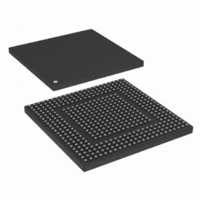
MPC8308VMAGD Freescale Semiconductor, MPC8308VMAGD Datasheet - Page 445

MPC8308VMAGD
Manufacturer Part Number
MPC8308VMAGD
Description
MPU POWERQUICC II PRO 473MAPBGA
Manufacturer
Freescale Semiconductor
Datasheets
1.MPC8308VMAGD.pdf
(90 pages)
2.MPC8308VMAGD.pdf
(2 pages)
3.MPC8308VMAGD.pdf
(1170 pages)
4.MPC8308VMAGD.pdf
(14 pages)
Specifications of MPC8308VMAGD
Processor Type
MPC83xx PowerQUICC II Pro 32-Bit
Speed
400MHz
Voltage
1V
Mounting Type
Surface Mount
Package / Case
473-MAPBGA
Product
Network Processor
Data Rate
256 bps
Frequency
400 MHz
Supply Voltage (max)
3.6 V
Supply Voltage (min)
3 V
Supply Current (max)
5 uA
Maximum Operating Temperature
+ 105 C
Minimum Operating Temperature
0 C
Interface
I2C, JTAG, SPI
Mounting Style
SMD/SMT
Lead Free Status / RoHS Status
Lead free / RoHS Compliant
Features
-
Lead Free Status / Rohs Status
Lead free / RoHS Compliant
Available stocks
Company
Part Number
Manufacturer
Quantity
Price
Company:
Part Number:
MPC8308VMAGD
Manufacturer:
FREESCAL
Quantity:
300
Company:
Part Number:
MPC8308VMAGD
Manufacturer:
Freescale Semiconductor
Quantity:
10 000
Part Number:
MPC8308VMAGD
Manufacturer:
FREESCALE
Quantity:
20 000
Company:
Part Number:
MPC8308VMAGD400/266
Manufacturer:
FREESCAL
Quantity:
300
Company:
Part Number:
MPC8308VMAGDA
Manufacturer:
Freescale Semiconductor
Quantity:
10 000
- MPC8308VMAGD PDF datasheet
- MPC8308VMAGD PDF datasheet #2
- MPC8308VMAGD PDF datasheet #3
- MPC8308VMAGD PDF datasheet #4
- Current page: 445 of 1170
- Download datasheet (9Mb)
The timing parameters are summarized in
10.4.3.3.5
Allowance for slow output driver turn-off when reading NAND Flash EEPROMs is made via setting of
ORn[EHTR] and ORn[TRLX]. The extended read data hold time, shown at t
Figure
LCSn is negated during t
10.4.3.4
Boot chip-select operation allows address decoding for a boot ROM before system initialization. LCS0 is
the boot chip-select output; its operation differs from other external chip-select outputs after a system reset.
Freescale Semiconductor
10-56, is a delay inserted by FCM between the last data read and another eLBC memory access.
FCM Boot Chip-Select Operation
FCM Extended Read Hold Timing
1
Option Register
TRLX
In the parameters, SCY refers to a delay of OR n [SCY] clock cycles.
(unused/internal)
LCLK
(unused)
LCS n
LFCLE/
LFALE
LFRE
LD[0:7]
TA
LALE
Figure 10-56. FCM Read Data Timing with Extended Hold Time
0
0
1
1
Attributes
MPC8308 PowerQUICC II Pro Processor Reference Manual, Rev. 0
(for TRLX = 0, EHTR = 1, RST = 1, SCY = 1, CLKDIV = 4*N)
EHTR
RST
Table 10-37. FCM Read Data Timing Parameters
0
1
0
1
to allow external devices and bus transceivers time to disable their drivers.
Notes:
½+2×SCY
1+2×SCY
¾+SCY
1+SCY
t
RP
t
t
RC
EHTR
Table
Timing Parameter (LCLK Clock Cycles)
= Read data cycle time.
read cycle
= Extended read data hold time.
last read data
t
RC
t
10-37.
RHT
1
1
2
2
2×SCY
2×SCY
SCY
SCY
t
WS
t
EHTR
3+2×SCY 8×(2+SCY)
3+2×SCY 8×(2+SCY)
2+SCY
2+SCY
t
RC
4×(2+SCY)
4×(2+SCY)
EHTR
1
t
WRT
Enhanced Local Bus Controller
in
Figure 10-45
and
10-65
Related parts for MPC8308VMAGD
Image
Part Number
Description
Manufacturer
Datasheet
Request
R
Part Number:
Description:
Development Boards & Kits - Other Processors MPC8308-NSG
Manufacturer:
Freescale Semiconductor
Datasheet:

Part Number:
Description:
MCU, MPU & DSP Development Tools For MPC8308 Ethernet USB I2C SPI
Manufacturer:
Freescale Semiconductor
Datasheet:

Part Number:
Description:
MCU, MPU & DSP Development Tools For MPC8308 Ethernet USB 32bit
Manufacturer:
Freescale Semiconductor
Datasheet:
Part Number:
Description:
Mpc8308 Powerquicc Ii Pro Processor Hardware Specification
Manufacturer:
Freescale Semiconductor, Inc
Datasheet:

Part Number:
Description:
BOARD REF DESIGN MPC8308
Manufacturer:
Freescale Semiconductor
Datasheet:

Part Number:
Description:
MPC8308 PowerQUICC II Pro Processor Hardware Specification
Manufacturer:
FREESCALE [Freescale Semiconductor, Inc]
Datasheet:
Part Number:
Description:
Microprocessors - MPU E300 ext tmp Qual266
Manufacturer:
Freescale Semiconductor
Datasheet:
Part Number:
Description:
Microprocessors - MPU E300 ext tmp Qual333
Manufacturer:
Freescale Semiconductor
Datasheet:
Part Number:
Description:
Microprocessors - MPU E300 EXT TEMP PB 400
Manufacturer:
Freescale Semiconductor
Datasheet:
Part Number:
Description:
Microprocessors - MPU E300 MP Pb 266
Manufacturer:
Freescale Semiconductor
Datasheet:
Part Number:
Description:
Microprocessors - MPU E300 MP Pb 400
Manufacturer:
Freescale Semiconductor
Datasheet:
Part Number:
Description:
Microprocessors - MPU E300 MP Pb 333
Manufacturer:
Freescale Semiconductor
Datasheet:
Part Number:
Description:
Manufacturer:
Freescale Semiconductor, Inc
Datasheet:
Part Number:
Description:
Manufacturer:
Freescale Semiconductor, Inc
Datasheet:
Part Number:
Description:
Manufacturer:
Freescale Semiconductor, Inc
Datasheet:


