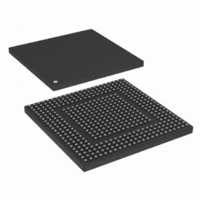
MPC8308VMAGD Freescale Semiconductor, MPC8308VMAGD Datasheet - Page 466

MPC8308VMAGD
Manufacturer Part Number
MPC8308VMAGD
Description
MPU POWERQUICC II PRO 473MAPBGA
Manufacturer
Freescale Semiconductor
Datasheets
1.MPC8308VMAGD.pdf
(90 pages)
2.MPC8308VMAGD.pdf
(2 pages)
3.MPC8308VMAGD.pdf
(1170 pages)
4.MPC8308VMAGD.pdf
(14 pages)
Specifications of MPC8308VMAGD
Processor Type
MPC83xx PowerQUICC II Pro 32-Bit
Speed
400MHz
Voltage
1V
Mounting Type
Surface Mount
Package / Case
473-MAPBGA
Product
Network Processor
Data Rate
256 bps
Frequency
400 MHz
Supply Voltage (max)
3.6 V
Supply Voltage (min)
3 V
Supply Current (max)
5 uA
Maximum Operating Temperature
+ 105 C
Minimum Operating Temperature
0 C
Interface
I2C, JTAG, SPI
Mounting Style
SMD/SMT
Lead Free Status / RoHS Status
Lead free / RoHS Compliant
Features
-
Lead Free Status / Rohs Status
Lead free / RoHS Compliant
Available stocks
Company
Part Number
Manufacturer
Quantity
Price
Company:
Part Number:
MPC8308VMAGD
Manufacturer:
FREESCAL
Quantity:
300
Company:
Part Number:
MPC8308VMAGD
Manufacturer:
Freescale Semiconductor
Quantity:
10 000
Part Number:
MPC8308VMAGD
Manufacturer:
FREESCALE
Quantity:
20 000
Company:
Part Number:
MPC8308VMAGD400/266
Manufacturer:
FREESCAL
Quantity:
300
Company:
Part Number:
MPC8308VMAGDA
Manufacturer:
Freescale Semiconductor
Quantity:
10 000
- MPC8308VMAGD PDF datasheet
- MPC8308VMAGD PDF datasheet #2
- MPC8308VMAGD PDF datasheet #3
- MPC8308VMAGD PDF datasheet #4
- Current page: 466 of 1170
- Download datasheet (9Mb)
Enhanced Local Bus Controller
conclusion of the sequence, eLBC will issue a command complete interrupt (LTESR[CC]) if interrupts are
enabled. MDR[AS3–AS0] then can be read to obtain the first 4 bytes of NAND Flash ID.
10.5.3.4
An example of configuring FCM to execute a random page read command to large-page NAND Flash is
shown in
buffer RAM, checking ECC as it proceeds. The sequence is initiated by writing FMR[OP] = 11, and
issuing a special operation to the bank. A few cycles before completion itself, FECCn gets updated with
the ECC bytes for the main region validated by FECCn[0]. At the conclusion of the sequence, eLBC will
issue a command complete interrupt (LTESR[CC]) if interrupts are enabled. Once the sequence has
completed, the shared buffer (buffer 1 for page index 5) and transfer error registers (LTECCR that reports
the 512 blocks with unibit /multibit errors if any) are valid.
10-86
Table
Register
FBCR
FBAR
FPAR
Register
FCR
FBCR
FBAR
FPAR
MDR
FCR
NAND Flash Page Read Command Sequence Example
FIR
10-46. This sequence reads an entire page (main and spare region) into the shared FCM
Table 10-46. FCM Register Settings for Page Read (OR n [PGS] = 1)
Table 10-45. FCM Register Settings for ID Read (OR n [PGS] = 1)
0x00005000 locates
(for example, block
MPC8308 PowerQUICC II Pro Processor Reference Manual, Rev. 0
page 5, buffer 1)
Initial Contents
Initial Contents
0x00010ab4)
(for example,
0x00300000
0x00000000
0x43BBBBB0
block index
page offset
0x90000000
0x00000000
—
—
—
CMD0 = 0x00 = random read address entry;
CMD1 = 0x30 = read page
BLK locates index of 128-Kbyte block
PI locates page index in BLK;
PI mod 2 indexes FCM buffer RAM;
MS = 0 and CI = 0
BC = 0 to read entire 2112-byte page with ECC check
CMD0 = 0x90 = read ID command; other commands unused
unused
unused
unused
AS0 = 0x00 = dummy address for read ID command;
AS0–AS3 return with first 4 bytes of ID code
OP0 = CM0 = command 0;
OP1 = UA = user address from MDR;
OP2–OP6 = RS = read 4 bytes ID into MDR[AS3–AS0];
OP7 = NOP
Description
Description
Freescale Semiconductor
Related parts for MPC8308VMAGD
Image
Part Number
Description
Manufacturer
Datasheet
Request
R
Part Number:
Description:
Development Boards & Kits - Other Processors MPC8308-NSG
Manufacturer:
Freescale Semiconductor
Datasheet:

Part Number:
Description:
MCU, MPU & DSP Development Tools For MPC8308 Ethernet USB I2C SPI
Manufacturer:
Freescale Semiconductor
Datasheet:

Part Number:
Description:
MCU, MPU & DSP Development Tools For MPC8308 Ethernet USB 32bit
Manufacturer:
Freescale Semiconductor
Datasheet:
Part Number:
Description:
Mpc8308 Powerquicc Ii Pro Processor Hardware Specification
Manufacturer:
Freescale Semiconductor, Inc
Datasheet:

Part Number:
Description:
BOARD REF DESIGN MPC8308
Manufacturer:
Freescale Semiconductor
Datasheet:

Part Number:
Description:
MPC8308 PowerQUICC II Pro Processor Hardware Specification
Manufacturer:
FREESCALE [Freescale Semiconductor, Inc]
Datasheet:
Part Number:
Description:
Microprocessors - MPU E300 ext tmp Qual266
Manufacturer:
Freescale Semiconductor
Datasheet:
Part Number:
Description:
Microprocessors - MPU E300 ext tmp Qual333
Manufacturer:
Freescale Semiconductor
Datasheet:
Part Number:
Description:
Microprocessors - MPU E300 EXT TEMP PB 400
Manufacturer:
Freescale Semiconductor
Datasheet:
Part Number:
Description:
Microprocessors - MPU E300 MP Pb 266
Manufacturer:
Freescale Semiconductor
Datasheet:
Part Number:
Description:
Microprocessors - MPU E300 MP Pb 400
Manufacturer:
Freescale Semiconductor
Datasheet:
Part Number:
Description:
Microprocessors - MPU E300 MP Pb 333
Manufacturer:
Freescale Semiconductor
Datasheet:
Part Number:
Description:
Manufacturer:
Freescale Semiconductor, Inc
Datasheet:
Part Number:
Description:
Manufacturer:
Freescale Semiconductor, Inc
Datasheet:
Part Number:
Description:
Manufacturer:
Freescale Semiconductor, Inc
Datasheet:


