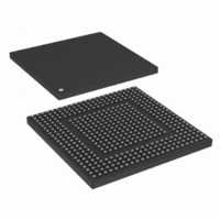
MPC8308VMAGD Freescale Semiconductor, MPC8308VMAGD Datasheet - Page 1074

MPC8308VMAGD
Manufacturer Part Number
MPC8308VMAGD
Description
MPU POWERQUICC II PRO 473MAPBGA
Manufacturer
Freescale Semiconductor
Datasheets
1.MPC8308VMAGD.pdf
(90 pages)
2.MPC8308VMAGD.pdf
(2 pages)
3.MPC8308VMAGD.pdf
(1170 pages)
4.MPC8308VMAGD.pdf
(14 pages)
Specifications of MPC8308VMAGD
Processor Type
MPC83xx PowerQUICC II Pro 32-Bit
Speed
400MHz
Voltage
1V
Mounting Type
Surface Mount
Package / Case
473-MAPBGA
Product
Network Processor
Data Rate
256 bps
Frequency
400 MHz
Supply Voltage (max)
3.6 V
Supply Voltage (min)
3 V
Supply Current (max)
5 uA
Maximum Operating Temperature
+ 105 C
Minimum Operating Temperature
0 C
Interface
I2C, JTAG, SPI
Mounting Style
SMD/SMT
Lead Free Status / RoHS Status
Lead free / RoHS Compliant
Features
-
Lead Free Status / Rohs Status
Lead free / RoHS Compliant
Available stocks
Company
Part Number
Manufacturer
Quantity
Price
Company:
Part Number:
MPC8308VMAGD
Manufacturer:
FREESCAL
Quantity:
300
Company:
Part Number:
MPC8308VMAGD
Manufacturer:
Freescale Semiconductor
Quantity:
10 000
Part Number:
MPC8308VMAGD
Manufacturer:
FREESCALE
Quantity:
20 000
Company:
Part Number:
MPC8308VMAGD400/266
Manufacturer:
FREESCAL
Quantity:
300
Company:
Part Number:
MPC8308VMAGDA
Manufacturer:
Freescale Semiconductor
Quantity:
10 000
- MPC8308VMAGD PDF datasheet
- MPC8308VMAGD PDF datasheet #2
- MPC8308VMAGD PDF datasheet #3
- MPC8308VMAGD PDF datasheet #4
- Current page: 1074 of 1170
- Download datasheet (9Mb)
I
broadcast message is the master address. Because the second byte is automatically acknowledged by
hardware, the receiver device software must verify that the broadcast message is intended for itself by
reading the second byte of the message. If the master address is for another receiver device and the third
byte is a write command, the software can ignore the third byte during the broadcast. If the master address
is for another receiver device and the third byte is a read command, software must write 0xFF to I2CDR
with I2CCR[TXAK] = 1 so that it does not interfere with the data written from the addressed device.
Each data byte is 8 bits long. Data bits can be changed only while SCL is low and must be held stable while
SCL is high, as shown in
significant bit (msb) is transmitted first. Each byte of data must be followed by an acknowledge bit, which
is signaled from the receiving device by pulling SDA low at the 9th clock. Therefore, one complete data
byte transfer takes 9 clock pulses. Several bytes can be transferred during a data transfer session.
If the slave receiver does not acknowledge the master, the SDA line must be left high by the slave. The
master can then generate a stop condition to abort the data transfer or a START condition (repeated
START) to begin a new calling.
If the master receiver does not acknowledge the slave transmitter after a byte of transmission, the slave
interprets that the end-of-data has been reached. Then the slave releases the SDA line for the master to
generate a STOP or a START condition.
17.4.1.3
Figure 17-8
terminate the previous transfer. The master uses this method to communicate with another slave or with
the same slave in a different mode (transmit/receive mode) without releasing the bus.
17.4.1.4
The master can terminate the transfer by generating a STOP condition to free the bus. A STOP condition
is defined as a low-to-high transition of the SDA signal while SCL is high. For more information, see
Figure
at which point the slave must release the bus. The STOP condition is initiated by a software write that
clears I2CCR[MSTA].
As described in
condition followed by a calling address without generating a STOP condition for the previous transfer.
This is called a repeated START condition.
17.4.1.5
The following sections give details about how aspects of the protocol are implemented in the I
17.4.1.5.1
The different conditions of the I
17-12
2
C Interface
•
•
17-8. Note that a master can generate a STOP even if the slave has transmitted an acknowledge bit,
START conditions are detected when an SDA fall occurs while SCL is high.
STOP conditions are detected when an SDA rise occurs while SCL is high.
shows a repeated START condition, which is generated without a STOP condition that can
Repeated START Condition
STOP Condition
Protocol Implementation Details
Transaction Monitoring—Implementation Details
Section 17.4.1.3, “Repeated START Condition,”
MPC8308 PowerQUICC II Pro Processor Reference Manual, Rev. 0
Figure
2
17-8. There is one clock pulse on SCL for each data bit, and the most
C data transfers are monitored as follows (see
the master can generate a START
Figure
Freescale Semiconductor
17-8):
2
C module.
Related parts for MPC8308VMAGD
Image
Part Number
Description
Manufacturer
Datasheet
Request
R
Part Number:
Description:
Development Boards & Kits - Other Processors MPC8308-NSG
Manufacturer:
Freescale Semiconductor
Datasheet:

Part Number:
Description:
MCU, MPU & DSP Development Tools For MPC8308 Ethernet USB I2C SPI
Manufacturer:
Freescale Semiconductor
Datasheet:

Part Number:
Description:
MCU, MPU & DSP Development Tools For MPC8308 Ethernet USB 32bit
Manufacturer:
Freescale Semiconductor
Datasheet:
Part Number:
Description:
Mpc8308 Powerquicc Ii Pro Processor Hardware Specification
Manufacturer:
Freescale Semiconductor, Inc
Datasheet:

Part Number:
Description:
BOARD REF DESIGN MPC8308
Manufacturer:
Freescale Semiconductor
Datasheet:

Part Number:
Description:
MPC8308 PowerQUICC II Pro Processor Hardware Specification
Manufacturer:
FREESCALE [Freescale Semiconductor, Inc]
Datasheet:
Part Number:
Description:
Microprocessors - MPU E300 ext tmp Qual266
Manufacturer:
Freescale Semiconductor
Datasheet:
Part Number:
Description:
Microprocessors - MPU E300 ext tmp Qual333
Manufacturer:
Freescale Semiconductor
Datasheet:
Part Number:
Description:
Microprocessors - MPU E300 EXT TEMP PB 400
Manufacturer:
Freescale Semiconductor
Datasheet:
Part Number:
Description:
Microprocessors - MPU E300 MP Pb 266
Manufacturer:
Freescale Semiconductor
Datasheet:
Part Number:
Description:
Microprocessors - MPU E300 MP Pb 400
Manufacturer:
Freescale Semiconductor
Datasheet:
Part Number:
Description:
Microprocessors - MPU E300 MP Pb 333
Manufacturer:
Freescale Semiconductor
Datasheet:
Part Number:
Description:
Manufacturer:
Freescale Semiconductor, Inc
Datasheet:
Part Number:
Description:
Manufacturer:
Freescale Semiconductor, Inc
Datasheet:
Part Number:
Description:
Manufacturer:
Freescale Semiconductor, Inc
Datasheet:


