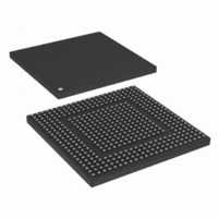
MPC8308VMAGD Freescale Semiconductor, MPC8308VMAGD Datasheet - Page 742

MPC8308VMAGD
Manufacturer Part Number
MPC8308VMAGD
Description
MPU POWERQUICC II PRO 473MAPBGA
Manufacturer
Freescale Semiconductor
Datasheets
1.MPC8308VMAGD.pdf
(90 pages)
2.MPC8308VMAGD.pdf
(2 pages)
3.MPC8308VMAGD.pdf
(1170 pages)
4.MPC8308VMAGD.pdf
(14 pages)
Specifications of MPC8308VMAGD
Processor Type
MPC83xx PowerQUICC II Pro 32-Bit
Speed
400MHz
Voltage
1V
Mounting Type
Surface Mount
Package / Case
473-MAPBGA
Product
Network Processor
Data Rate
256 bps
Frequency
400 MHz
Supply Voltage (max)
3.6 V
Supply Voltage (min)
3 V
Supply Current (max)
5 uA
Maximum Operating Temperature
+ 105 C
Minimum Operating Temperature
0 C
Interface
I2C, JTAG, SPI
Mounting Style
SMD/SMT
Lead Free Status / RoHS Status
Lead free / RoHS Compliant
Features
-
Lead Free Status / Rohs Status
Lead free / RoHS Compliant
Available stocks
Company
Part Number
Manufacturer
Quantity
Price
Company:
Part Number:
MPC8308VMAGD
Manufacturer:
FREESCAL
Quantity:
300
Company:
Part Number:
MPC8308VMAGD
Manufacturer:
Freescale Semiconductor
Quantity:
10 000
Part Number:
MPC8308VMAGD
Manufacturer:
FREESCALE
Quantity:
20 000
Company:
Part Number:
MPC8308VMAGD400/266
Manufacturer:
FREESCAL
Quantity:
300
Company:
Part Number:
MPC8308VMAGDA
Manufacturer:
Freescale Semiconductor
Quantity:
10 000
- MPC8308VMAGD PDF datasheet
- MPC8308VMAGD PDF datasheet #2
- MPC8308VMAGD PDF datasheet #3
- MPC8308VMAGD PDF datasheet #4
- Current page: 742 of 1170
- Download datasheet (9Mb)
PCI Express Interface Controller
14.1.3
The following is a list of PCI Express controller features:
14.1.4
This section describes how some parameters that affect the PCI Express controller operating modes are
determined by dedicated memory mapped registers.
14.1.4.1
The PCI Express controller can function as either a root complex (RC) or an endpoint (EP) device. The
PCI Express control registers 1 and 2 determine the RC/EP mode; see
Control Registers
14.1.4.2
The link width of the PCI Express controller is ×1.
14-4
•
•
•
•
•
•
•
•
•
•
•
•
•
•
•
•
•
•
•
•
•
Designed to be compatible with the PCI Express Base Specification, Version 1.0a
Root complex (RC) and endpoint (EP) configurations
32- and 64-bit address support
PCI Express link of ×1 lane
Access to all PCI Express memory
Access to I/O address spaces as requestor only in RC mode
Posting of processor-to-PCI Express and PCI Express-to-memory writes
Strong and relaxed transaction ordering rules
PCI Express configuration registers
Baseline and advanced error reporting
One virtual channel (VC0)
128-byte maximum payload size (Max_Payload_Size) for memory read and write operations
Four inbound general-purpose translation windows
Four outbound translation windows
Up to four outstanding PCI Express transactions from each controller (posted or non-posted)
Credit-based flow control management
PCI Express messages and interrupts
Maximum 32-byte payload transactions from the CSB
Interrupt generation from messages or upon detection of errors
Read and Write DMA engines
Support polarity inversion
Features
Modes of Operation
Root Complex/Endpoint Modes
Link Width
(PECR1).”
MPC8308 PowerQUICC II Pro Processor Reference Manual, Rev. 0
Section 5.2.2.11, “PCI Express
Freescale Semiconductor
Related parts for MPC8308VMAGD
Image
Part Number
Description
Manufacturer
Datasheet
Request
R
Part Number:
Description:
Development Boards & Kits - Other Processors MPC8308-NSG
Manufacturer:
Freescale Semiconductor
Datasheet:

Part Number:
Description:
MCU, MPU & DSP Development Tools For MPC8308 Ethernet USB I2C SPI
Manufacturer:
Freescale Semiconductor
Datasheet:

Part Number:
Description:
MCU, MPU & DSP Development Tools For MPC8308 Ethernet USB 32bit
Manufacturer:
Freescale Semiconductor
Datasheet:
Part Number:
Description:
Mpc8308 Powerquicc Ii Pro Processor Hardware Specification
Manufacturer:
Freescale Semiconductor, Inc
Datasheet:

Part Number:
Description:
BOARD REF DESIGN MPC8308
Manufacturer:
Freescale Semiconductor
Datasheet:

Part Number:
Description:
MPC8308 PowerQUICC II Pro Processor Hardware Specification
Manufacturer:
FREESCALE [Freescale Semiconductor, Inc]
Datasheet:
Part Number:
Description:
Microprocessors - MPU E300 ext tmp Qual266
Manufacturer:
Freescale Semiconductor
Datasheet:
Part Number:
Description:
Microprocessors - MPU E300 ext tmp Qual333
Manufacturer:
Freescale Semiconductor
Datasheet:
Part Number:
Description:
Microprocessors - MPU E300 EXT TEMP PB 400
Manufacturer:
Freescale Semiconductor
Datasheet:
Part Number:
Description:
Microprocessors - MPU E300 MP Pb 266
Manufacturer:
Freescale Semiconductor
Datasheet:
Part Number:
Description:
Microprocessors - MPU E300 MP Pb 400
Manufacturer:
Freescale Semiconductor
Datasheet:
Part Number:
Description:
Microprocessors - MPU E300 MP Pb 333
Manufacturer:
Freescale Semiconductor
Datasheet:
Part Number:
Description:
Manufacturer:
Freescale Semiconductor, Inc
Datasheet:
Part Number:
Description:
Manufacturer:
Freescale Semiconductor, Inc
Datasheet:
Part Number:
Description:
Manufacturer:
Freescale Semiconductor, Inc
Datasheet:


