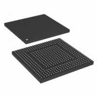
MPC8308VMAGD Freescale Semiconductor, MPC8308VMAGD Datasheet - Page 261

MPC8308VMAGD
Manufacturer Part Number
MPC8308VMAGD
Description
MPU POWERQUICC II PRO 473MAPBGA
Manufacturer
Freescale Semiconductor
Datasheets
1.MPC8308VMAGD.pdf
(90 pages)
2.MPC8308VMAGD.pdf
(2 pages)
3.MPC8308VMAGD.pdf
(1170 pages)
4.MPC8308VMAGD.pdf
(14 pages)
Specifications of MPC8308VMAGD
Processor Type
MPC83xx PowerQUICC II Pro 32-Bit
Speed
400MHz
Voltage
1V
Mounting Type
Surface Mount
Package / Case
473-MAPBGA
Product
Network Processor
Data Rate
256 bps
Frequency
400 MHz
Supply Voltage (max)
3.6 V
Supply Voltage (min)
3 V
Supply Current (max)
5 uA
Maximum Operating Temperature
+ 105 C
Minimum Operating Temperature
0 C
Interface
I2C, JTAG, SPI
Mounting Style
SMD/SMT
Lead Free Status / RoHS Status
Lead free / RoHS Compliant
Features
-
Lead Free Status / Rohs Status
Lead free / RoHS Compliant
Available stocks
Company
Part Number
Manufacturer
Quantity
Price
Company:
Part Number:
MPC8308VMAGD
Manufacturer:
FREESCAL
Quantity:
300
Company:
Part Number:
MPC8308VMAGD
Manufacturer:
Freescale Semiconductor
Quantity:
10 000
Part Number:
MPC8308VMAGD
Manufacturer:
FREESCALE
Quantity:
20 000
Company:
Part Number:
MPC8308VMAGD400/266
Manufacturer:
FREESCAL
Quantity:
300
Company:
Part Number:
MPC8308VMAGDA
Manufacturer:
Freescale Semiconductor
Quantity:
10 000
- MPC8308VMAGD PDF datasheet
- MPC8308VMAGD PDF datasheet #2
- MPC8308VMAGD PDF datasheet #3
- MPC8308VMAGD PDF datasheet #4
- Current page: 261 of 1170
- Download datasheet (9Mb)
7.4.3
The following sections describe the general cache characteristics as implemented in the PowerPC
architecture and the core implementation.
7.4.3.1
The PowerPC architecture does not define hardware aspects of cache implementations. The e300 core
controls the following memory access modes on a page or block basis:
Note that in the core, a cache block is defined as eight words. The VEA defines cache management
instructions that provide a means by which the application programmer can affect the cache contents.
7.4.3.2
The e300c3 provides 16-Kbyte, four-way set-associative instruction and data caches. The caches are
physically addressed, and the data cache can operate in either write-back or write-through mode as
specified by the PowerPC architecture.
The data cache is configured as 128 sets of 4 blocks each on the e300c3. Each block consists of 32 bytes,
2 state bits, and an address tag. The two state bits implement the three-state MEI
(modified/exclusive/invalid) protocol. Each block contains eight 32-bit words. Note that the PowerPC
architecture defines the term ‘block’ as the cacheable unit. For the core, the block size is equivalent to a
cache line. A block diagram of the data cache organization is shown in
The instruction cache is configured as 128 sets of 4 blocks each on the e300c3. Each block consists of
32 bytes, an address tag, and a valid bit. The instruction cache may not be written to, except through a
block fill operation. In the e300 core, the instruction cache is blocked only until the critical load completes.
The e300 core supports instruction fetching from other instruction cache lines following the forwarding of
the critical-first-double-word of a cache line load operation. Successive instruction fetches from the cache
line being loaded are forwarded, and accesses to other instruction cache lines can proceed during the cache
line load operation. The instruction cache is not snooped, and cache coherency must be maintained by
software. A fast hardware invalidation capability is provided to support cache maintenance.
Freescale Semiconductor
•
•
•
Write-back/write-through mode
Caching-inhibited mode
Memory coherency
Cache Implementation
PowerPC Cache Characteristics
Implementation-Specific Cache Organization
MPC8308 PowerQUICC II Pro Processor Reference Manual, Rev. 0
Figure
7-3.
e300 Processor Core Overview
7-29
Related parts for MPC8308VMAGD
Image
Part Number
Description
Manufacturer
Datasheet
Request
R
Part Number:
Description:
Development Boards & Kits - Other Processors MPC8308-NSG
Manufacturer:
Freescale Semiconductor
Datasheet:

Part Number:
Description:
MCU, MPU & DSP Development Tools For MPC8308 Ethernet USB I2C SPI
Manufacturer:
Freescale Semiconductor
Datasheet:

Part Number:
Description:
MCU, MPU & DSP Development Tools For MPC8308 Ethernet USB 32bit
Manufacturer:
Freescale Semiconductor
Datasheet:
Part Number:
Description:
Mpc8308 Powerquicc Ii Pro Processor Hardware Specification
Manufacturer:
Freescale Semiconductor, Inc
Datasheet:

Part Number:
Description:
BOARD REF DESIGN MPC8308
Manufacturer:
Freescale Semiconductor
Datasheet:

Part Number:
Description:
MPC8308 PowerQUICC II Pro Processor Hardware Specification
Manufacturer:
FREESCALE [Freescale Semiconductor, Inc]
Datasheet:
Part Number:
Description:
Microprocessors - MPU E300 ext tmp Qual266
Manufacturer:
Freescale Semiconductor
Datasheet:
Part Number:
Description:
Microprocessors - MPU E300 ext tmp Qual333
Manufacturer:
Freescale Semiconductor
Datasheet:
Part Number:
Description:
Microprocessors - MPU E300 EXT TEMP PB 400
Manufacturer:
Freescale Semiconductor
Datasheet:
Part Number:
Description:
Microprocessors - MPU E300 MP Pb 266
Manufacturer:
Freescale Semiconductor
Datasheet:
Part Number:
Description:
Microprocessors - MPU E300 MP Pb 400
Manufacturer:
Freescale Semiconductor
Datasheet:
Part Number:
Description:
Microprocessors - MPU E300 MP Pb 333
Manufacturer:
Freescale Semiconductor
Datasheet:
Part Number:
Description:
Manufacturer:
Freescale Semiconductor, Inc
Datasheet:
Part Number:
Description:
Manufacturer:
Freescale Semiconductor, Inc
Datasheet:
Part Number:
Description:
Manufacturer:
Freescale Semiconductor, Inc
Datasheet:


