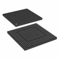
MPC8308VMAGD Freescale Semiconductor, MPC8308VMAGD Datasheet - Page 1106

MPC8308VMAGD
Manufacturer Part Number
MPC8308VMAGD
Description
MPU POWERQUICC II PRO 473MAPBGA
Manufacturer
Freescale Semiconductor
Datasheets
1.MPC8308VMAGD.pdf
(90 pages)
2.MPC8308VMAGD.pdf
(2 pages)
3.MPC8308VMAGD.pdf
(1170 pages)
4.MPC8308VMAGD.pdf
(14 pages)
Specifications of MPC8308VMAGD
Processor Type
MPC83xx PowerQUICC II Pro 32-Bit
Speed
400MHz
Voltage
1V
Mounting Type
Surface Mount
Package / Case
473-MAPBGA
Product
Network Processor
Data Rate
256 bps
Frequency
400 MHz
Supply Voltage (max)
3.6 V
Supply Voltage (min)
3 V
Supply Current (max)
5 uA
Maximum Operating Temperature
+ 105 C
Minimum Operating Temperature
0 C
Interface
I2C, JTAG, SPI
Mounting Style
SMD/SMT
Lead Free Status / RoHS Status
Lead free / RoHS Compliant
Features
-
Lead Free Status / Rohs Status
Lead free / RoHS Compliant
Available stocks
Company
Part Number
Manufacturer
Quantity
Price
Company:
Part Number:
MPC8308VMAGD
Manufacturer:
FREESCAL
Quantity:
300
Company:
Part Number:
MPC8308VMAGD
Manufacturer:
Freescale Semiconductor
Quantity:
10 000
Part Number:
MPC8308VMAGD
Manufacturer:
FREESCALE
Quantity:
20 000
Company:
Part Number:
MPC8308VMAGD400/266
Manufacturer:
FREESCAL
Quantity:
300
Company:
Part Number:
MPC8308VMAGDA
Manufacturer:
Freescale Semiconductor
Quantity:
10 000
- MPC8308VMAGD PDF datasheet
- MPC8308VMAGD PDF datasheet #2
- MPC8308VMAGD PDF datasheet #3
- MPC8308VMAGD PDF datasheet #4
- Current page: 1106 of 1170
- Download datasheet (9Mb)
DUART
18.4.1.2
Each data transfer contains 5, 6, 7, or 8 bits of data. The ULCR data bit length for the transmitter and
receiver UART devices must agree before a transfer begins; otherwise, a parity or framing error may occur.
A transfer begins when UTHR is written. At that time, a START bit is generated followed by 5 to 8 of the
data bits previously written to the UTHR. The data bits are driven from the least- to the most-significant
bits. After the parity and STOP bits, a new data transfer can begin if new data is written to UTHR.
18.4.1.3
The user has the option of using even, odd, no parity, or stick parity (see
Registers (ULCR1 and ULCR2).”
transferring data. When receiving data, a parity error can occur if an unexpected parity value is detected
(see
18.4.1.4
The transmitter device ends the write transfer by generating a STOP bit. The STOP bit is always high. The
user can program the length of the STOP bit(s) in the ULCR. Both the receiver and transmitter STOP bit
length must agree before attempting to transfer data. A framing error can occur if an invalid STOP bit is
detected.
18.4.2
Each UART contains an independent programmable baud-rate generator, that is capable of taking the
system clock input and dividing the input by any divisor from 1 to 2
The baud rate is defined as the number of bits per second that can be sent over the UART bus. The formula
for calculating baud rate is as follows:
Therefore, the output frequency of the baud-rate generator is 16 times the baud rate.
The divisor value is determined by the following two 8-bit registers to form a 16-bit binary number:
Upon loading either of the divisor latches, a 16-bit baud-rate counter is loaded.
The divisor latches must be loaded during initialization to ensure proper operation of the baud-rate
generator. Both UART devices on the same bus must be programmed for the same baud rate before starting
a transfer.
The baud clock can be passed to the performance monitor by enabling UAFR[BO]. This can be used to
determine baud-rate errors.
18-18
•
•
Section 18.3.1.9, “Line Status Registers (ULSR1 and
UART divisor most significant byte register (UDMB)
UART divisor least significant byte register (UDLB)
Baud-Rate Generator Logic
Data Transfer
Parity Bit
STOP Bit
Baud rate = (1/16) × (system clock frequency/divisor value)
MPC8308 PowerQUICC II Pro Processor Reference Manual, Rev. 0
Both the receiver and transmitter parity definitions must agree before
ULSR2)”).
16
– 1.
Section 18.3.1.7, “Line Control
Freescale Semiconductor
Eqn. 18-1
Related parts for MPC8308VMAGD
Image
Part Number
Description
Manufacturer
Datasheet
Request
R
Part Number:
Description:
Development Boards & Kits - Other Processors MPC8308-NSG
Manufacturer:
Freescale Semiconductor
Datasheet:

Part Number:
Description:
MCU, MPU & DSP Development Tools For MPC8308 Ethernet USB I2C SPI
Manufacturer:
Freescale Semiconductor
Datasheet:

Part Number:
Description:
MCU, MPU & DSP Development Tools For MPC8308 Ethernet USB 32bit
Manufacturer:
Freescale Semiconductor
Datasheet:
Part Number:
Description:
Mpc8308 Powerquicc Ii Pro Processor Hardware Specification
Manufacturer:
Freescale Semiconductor, Inc
Datasheet:

Part Number:
Description:
BOARD REF DESIGN MPC8308
Manufacturer:
Freescale Semiconductor
Datasheet:

Part Number:
Description:
MPC8308 PowerQUICC II Pro Processor Hardware Specification
Manufacturer:
FREESCALE [Freescale Semiconductor, Inc]
Datasheet:
Part Number:
Description:
Microprocessors - MPU E300 ext tmp Qual266
Manufacturer:
Freescale Semiconductor
Datasheet:
Part Number:
Description:
Microprocessors - MPU E300 ext tmp Qual333
Manufacturer:
Freescale Semiconductor
Datasheet:
Part Number:
Description:
Microprocessors - MPU E300 EXT TEMP PB 400
Manufacturer:
Freescale Semiconductor
Datasheet:
Part Number:
Description:
Microprocessors - MPU E300 MP Pb 266
Manufacturer:
Freescale Semiconductor
Datasheet:
Part Number:
Description:
Microprocessors - MPU E300 MP Pb 400
Manufacturer:
Freescale Semiconductor
Datasheet:
Part Number:
Description:
Microprocessors - MPU E300 MP Pb 333
Manufacturer:
Freescale Semiconductor
Datasheet:
Part Number:
Description:
Manufacturer:
Freescale Semiconductor, Inc
Datasheet:
Part Number:
Description:
Manufacturer:
Freescale Semiconductor, Inc
Datasheet:
Part Number:
Description:
Manufacturer:
Freescale Semiconductor, Inc
Datasheet:


