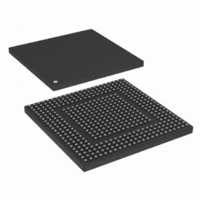
MPC8308VMAGD Freescale Semiconductor, MPC8308VMAGD Datasheet - Page 892

MPC8308VMAGD
Manufacturer Part Number
MPC8308VMAGD
Description
MPU POWERQUICC II PRO 473MAPBGA
Manufacturer
Freescale Semiconductor
Datasheets
1.MPC8308VMAGD.pdf
(90 pages)
2.MPC8308VMAGD.pdf
(2 pages)
3.MPC8308VMAGD.pdf
(1170 pages)
4.MPC8308VMAGD.pdf
(14 pages)
Specifications of MPC8308VMAGD
Processor Type
MPC83xx PowerQUICC II Pro 32-Bit
Speed
400MHz
Voltage
1V
Mounting Type
Surface Mount
Package / Case
473-MAPBGA
Product
Network Processor
Data Rate
256 bps
Frequency
400 MHz
Supply Voltage (max)
3.6 V
Supply Voltage (min)
3 V
Supply Current (max)
5 uA
Maximum Operating Temperature
+ 105 C
Minimum Operating Temperature
0 C
Interface
I2C, JTAG, SPI
Mounting Style
SMD/SMT
Lead Free Status / RoHS Status
Lead free / RoHS Compliant
Features
-
Lead Free Status / Rohs Status
Lead free / RoHS Compliant
Available stocks
Company
Part Number
Manufacturer
Quantity
Price
Company:
Part Number:
MPC8308VMAGD
Manufacturer:
FREESCAL
Quantity:
300
Company:
Part Number:
MPC8308VMAGD
Manufacturer:
Freescale Semiconductor
Quantity:
10 000
Part Number:
MPC8308VMAGD
Manufacturer:
FREESCALE
Quantity:
20 000
Company:
Part Number:
MPC8308VMAGD400/266
Manufacturer:
FREESCAL
Quantity:
300
Company:
Part Number:
MPC8308VMAGDA
Manufacturer:
Freescale Semiconductor
Quantity:
10 000
- MPC8308VMAGD PDF datasheet
- MPC8308VMAGD PDF datasheet #2
- MPC8308VMAGD PDF datasheet #3
- MPC8308VMAGD PDF datasheet #4
- Current page: 892 of 1170
- Download datasheet (9Mb)
Enhanced Three-Speed Ethernet Controllers
16-8
TSEC_GTX_CLK125
TSEC n _GTX_CLK
TSEC n _RXD[3:0]
TSEC n _RX_CLK
TSEC n _TX_CLK
TSEC n _RX_DV
TSEC n _RX_ER
TSEC_MDIO
TSEC_MDC
Signal
Table 16-2. eTSEC Signals—Detailed Signal Descriptions (continued)
I/O
I/O Management data input/output.
O
O
I
I
I
I
I
I
MPC8308 PowerQUICC II Pro Processor Reference Manual, Rev. 0
Gigabit transmit clock. This signal is an output from the eTSEC into the PHY.
In RGMII mode, TSEC n _GTX_CLK becomes the transmit clock and provides timing reference
during 1000Base-T (125 MHz), 100Base-T (25 MHz) and 10Base-T (2.5 MHz) transmissions.
This signal feeds back the uninverted transmit clock in MII mode, but feeds back an inverted
transmit clock in RGMII mode.
This signal is driven low unless transmission is enabled.
Gigabit transmit 125-MHz source. This signal must be generated externally with a crystal or
oscillator, or is sometimes provided by the PHY. TSEC_GTX_CLK125 is a 125-MHz input into the
eTSEC and is used to generate all 125-MHz related signals and clocks in the RGMII mode.
This input is not used in the MII mode.
Management data clock.
This signal is a clock (typically 2.5 MHz) supplied by the MAC
(IEEE set minimum period of 400 ns or a frequency of 2.5 MHz, but the device may be configured
up to 12.5 MHz if supported by the PHY at that speed.) The frequency can be modified by writing
to MIIMCFG[28:31] of the eTSEC1 controller.
Receive clock. In MII or RGMII mode, the receive clock TSEC n _RX_CLK is a continuous clock
(2.5, 25, or 125 MHz) that provides a timing reference for TSEC n _RX_DV, TSEC n _RXD, and
TSEC n _RX_ER.
Receive data valid. In MII mode, if TSEC n _RX_DV is asserted, the PHY is indicating that valid
data is present on the MII interface.
In RGMII mode, TSEC n _RX_DV becomes RX_CTL. The RX_DV and RX_ERR are received on
this signal on the rising and falling edges of TSEC n _RX_CLK.
Receive data in. In MII mode, TSEC n _RXD[3:0] represents a nibble of data to be transferred from
the PHY to the MAC when TSEC n _RX_DV is asserted. A completely-formed SFD must be
passed across the MII. While TSEC n _RX_DV is not asserted, TSEC n _RXD has no meaning.
In RGMII mode, data bits 3–0 are received on the rising edge of TSEC n _RX_CLK and data bits
7–4 are received on the falling edge of TSEC n _RX_CLK.
Receive error
Transmit clock in. In MII mode, TSEC n _TX_CLK is a continuous clock (2.5 or 25 MHz) that
provides a timing reference for the TSEC n _TX_EN, TSEC n _TXD, and TSEC n _TX_ER signals.
This signal is not used in the eTSEC RGMII mode.
Meaning
Meaning
Timing Asserted/Negated—This signal is required to be synchronous with the TSEC_MDC
State
State
Asserted/Negated—TSEC_MDIO is a bidirectional signal to input PHY-supplied status
Asserted/Negated—In MII mode, if TSEC n _RX_ER and TSEC n _RX_DV are asserted,
during management read cycles and output control during MII management write
cycles. Addressed using eTSEC1 memory-mapped registers.
signal.
the PHY has detected an error in the current frame.
This signal is not used in the RGMII mode.
Description
Freescale Semiconductor
Related parts for MPC8308VMAGD
Image
Part Number
Description
Manufacturer
Datasheet
Request
R
Part Number:
Description:
Development Boards & Kits - Other Processors MPC8308-NSG
Manufacturer:
Freescale Semiconductor
Datasheet:

Part Number:
Description:
MCU, MPU & DSP Development Tools For MPC8308 Ethernet USB I2C SPI
Manufacturer:
Freescale Semiconductor
Datasheet:

Part Number:
Description:
MCU, MPU & DSP Development Tools For MPC8308 Ethernet USB 32bit
Manufacturer:
Freescale Semiconductor
Datasheet:
Part Number:
Description:
Mpc8308 Powerquicc Ii Pro Processor Hardware Specification
Manufacturer:
Freescale Semiconductor, Inc
Datasheet:

Part Number:
Description:
BOARD REF DESIGN MPC8308
Manufacturer:
Freescale Semiconductor
Datasheet:

Part Number:
Description:
MPC8308 PowerQUICC II Pro Processor Hardware Specification
Manufacturer:
FREESCALE [Freescale Semiconductor, Inc]
Datasheet:
Part Number:
Description:
Microprocessors - MPU E300 ext tmp Qual266
Manufacturer:
Freescale Semiconductor
Datasheet:
Part Number:
Description:
Microprocessors - MPU E300 ext tmp Qual333
Manufacturer:
Freescale Semiconductor
Datasheet:
Part Number:
Description:
Microprocessors - MPU E300 EXT TEMP PB 400
Manufacturer:
Freescale Semiconductor
Datasheet:
Part Number:
Description:
Microprocessors - MPU E300 MP Pb 266
Manufacturer:
Freescale Semiconductor
Datasheet:
Part Number:
Description:
Microprocessors - MPU E300 MP Pb 400
Manufacturer:
Freescale Semiconductor
Datasheet:
Part Number:
Description:
Microprocessors - MPU E300 MP Pb 333
Manufacturer:
Freescale Semiconductor
Datasheet:
Part Number:
Description:
Manufacturer:
Freescale Semiconductor, Inc
Datasheet:
Part Number:
Description:
Manufacturer:
Freescale Semiconductor, Inc
Datasheet:
Part Number:
Description:
Manufacturer:
Freescale Semiconductor, Inc
Datasheet:


