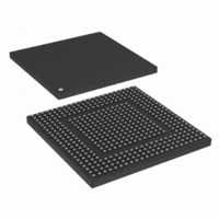
MPC8308VMAGD Freescale Semiconductor, MPC8308VMAGD Datasheet - Page 807

MPC8308VMAGD
Manufacturer Part Number
MPC8308VMAGD
Description
MPU POWERQUICC II PRO 473MAPBGA
Manufacturer
Freescale Semiconductor
Datasheets
1.MPC8308VMAGD.pdf
(90 pages)
2.MPC8308VMAGD.pdf
(2 pages)
3.MPC8308VMAGD.pdf
(1170 pages)
4.MPC8308VMAGD.pdf
(14 pages)
Specifications of MPC8308VMAGD
Processor Type
MPC83xx PowerQUICC II Pro 32-Bit
Speed
400MHz
Voltage
1V
Mounting Type
Surface Mount
Package / Case
473-MAPBGA
Product
Network Processor
Data Rate
256 bps
Frequency
400 MHz
Supply Voltage (max)
3.6 V
Supply Voltage (min)
3 V
Supply Current (max)
5 uA
Maximum Operating Temperature
+ 105 C
Minimum Operating Temperature
0 C
Interface
I2C, JTAG, SPI
Mounting Style
SMD/SMT
Lead Free Status / RoHS Status
Lead free / RoHS Compliant
Features
-
Lead Free Status / Rohs Status
Lead free / RoHS Compliant
Available stocks
Company
Part Number
Manufacturer
Quantity
Price
Company:
Part Number:
MPC8308VMAGD
Manufacturer:
FREESCAL
Quantity:
300
Company:
Part Number:
MPC8308VMAGD
Manufacturer:
Freescale Semiconductor
Quantity:
10 000
Part Number:
MPC8308VMAGD
Manufacturer:
FREESCALE
Quantity:
20 000
Company:
Part Number:
MPC8308VMAGD400/266
Manufacturer:
FREESCAL
Quantity:
300
Company:
Part Number:
MPC8308VMAGDA
Manufacturer:
Freescale Semiconductor
Quantity:
10 000
- MPC8308VMAGD PDF datasheet
- MPC8308VMAGD PDF datasheet #2
- MPC8308VMAGD PDF datasheet #3
- MPC8308VMAGD PDF datasheet #4
- Current page: 807 of 1170
- Download datasheet (9Mb)
The fields of the PCI Express Device Capabilities Update Register are described in
14.4.6.10 PCI Express Link Capabilities Update Register
The PCI Express link capabilities update register shown in
Express link capabilities register in the PCI Express configuration header (offset 0x58). It can be used
when the device is configured as an End Point to make the correct link information available to the
Freescale Semiconductor
Offset 0x47C
Reset 0 0 0 0 0 0 0 0 0 0 0 0 0 0 0 0 0
31–15
11–9
Bits
8–6
4–3
2–0
14
13
12
5
W
R
31
Table 14-83. PCI Express Device Capabilities Update Register Fields Description
L0SAL
Name
MPLS
(PEX_LINKCAP_UPDATE)
L1AL
APB
PIP
AIP
—
—
—
Figure 14-85. PCI Express Device Capabilities Update Register
Reserved
Power Indicator Present
Attention Indicator Present
Attention Button Present
Endpoint L1 Acceptable Latency. This field indicates the acceptable latency that an Endpoint can
withstand due to the transition from L1 state to the L0 state. Defined encodings are:
000b Less than 1us
001b 1 μs to less than 2 μs
010b 2 μs to less than 4 μs
011b 4 μs to less than 8 μs
100b 8 μs to less than 16 μs
101b 16 μs to less than 32 μs
110b 32 μs-64 ìs
111b More than 64 μs
Endpoint L0s Acceptable Latency. This field indicates the acceptable total latency that an Endpoint
can withstand due to the transition from L0s state to the L0 state. Defined encodings are:
000b Less than 64 ns
001b 64 ns to less than 128 ns
010b 128 ns to less than 256 ns
011b 256 ns to less than 512 ns
100b 512 ns to less than 1 μs
101b 1 μs to less than 2 μs
110b 2 μs-4 μs
111b More than 4 μs
Reserved (Extended Tag Field Supported). Must be set to 0b.
Reserved (Phantom Functions Supported). Must be set to 00b.
Max Payload Size Supported. Must be set to 000b (128bytes)
MPC8308 PowerQUICC II Pro Processor Reference Manual, Rev. 0
—
PIP AIP APB
14
0
Figure 14-86
Description
13
0
12
0
11
0
L1AL
is used to set the values to the PCI
0
0
9
0
8
L0SAL
PCI Express Interface Controller
0
Table
0 0 0 0 0
6
5
14-83.
4
Access: R/W
3
2
MPLS
0
14-69
0
0
Related parts for MPC8308VMAGD
Image
Part Number
Description
Manufacturer
Datasheet
Request
R
Part Number:
Description:
Development Boards & Kits - Other Processors MPC8308-NSG
Manufacturer:
Freescale Semiconductor
Datasheet:

Part Number:
Description:
MCU, MPU & DSP Development Tools For MPC8308 Ethernet USB I2C SPI
Manufacturer:
Freescale Semiconductor
Datasheet:

Part Number:
Description:
MCU, MPU & DSP Development Tools For MPC8308 Ethernet USB 32bit
Manufacturer:
Freescale Semiconductor
Datasheet:
Part Number:
Description:
Mpc8308 Powerquicc Ii Pro Processor Hardware Specification
Manufacturer:
Freescale Semiconductor, Inc
Datasheet:

Part Number:
Description:
BOARD REF DESIGN MPC8308
Manufacturer:
Freescale Semiconductor
Datasheet:

Part Number:
Description:
MPC8308 PowerQUICC II Pro Processor Hardware Specification
Manufacturer:
FREESCALE [Freescale Semiconductor, Inc]
Datasheet:
Part Number:
Description:
Microprocessors - MPU E300 ext tmp Qual266
Manufacturer:
Freescale Semiconductor
Datasheet:
Part Number:
Description:
Microprocessors - MPU E300 ext tmp Qual333
Manufacturer:
Freescale Semiconductor
Datasheet:
Part Number:
Description:
Microprocessors - MPU E300 EXT TEMP PB 400
Manufacturer:
Freescale Semiconductor
Datasheet:
Part Number:
Description:
Microprocessors - MPU E300 MP Pb 266
Manufacturer:
Freescale Semiconductor
Datasheet:
Part Number:
Description:
Microprocessors - MPU E300 MP Pb 400
Manufacturer:
Freescale Semiconductor
Datasheet:
Part Number:
Description:
Microprocessors - MPU E300 MP Pb 333
Manufacturer:
Freescale Semiconductor
Datasheet:
Part Number:
Description:
Manufacturer:
Freescale Semiconductor, Inc
Datasheet:
Part Number:
Description:
Manufacturer:
Freescale Semiconductor, Inc
Datasheet:
Part Number:
Description:
Manufacturer:
Freescale Semiconductor, Inc
Datasheet:


