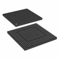
MPC8308VMAGD Freescale Semiconductor, MPC8308VMAGD Datasheet - Page 1119

MPC8308VMAGD
Manufacturer Part Number
MPC8308VMAGD
Description
MPU POWERQUICC II PRO 473MAPBGA
Manufacturer
Freescale Semiconductor
Datasheets
1.MPC8308VMAGD.pdf
(90 pages)
2.MPC8308VMAGD.pdf
(2 pages)
3.MPC8308VMAGD.pdf
(1170 pages)
4.MPC8308VMAGD.pdf
(14 pages)
Specifications of MPC8308VMAGD
Processor Type
MPC83xx PowerQUICC II Pro 32-Bit
Speed
400MHz
Voltage
1V
Mounting Type
Surface Mount
Package / Case
473-MAPBGA
Product
Network Processor
Data Rate
256 bps
Frequency
400 MHz
Supply Voltage (max)
3.6 V
Supply Voltage (min)
3 V
Supply Current (max)
5 uA
Maximum Operating Temperature
+ 105 C
Minimum Operating Temperature
0 C
Interface
I2C, JTAG, SPI
Mounting Style
SMD/SMT
Lead Free Status / RoHS Status
Lead free / RoHS Compliant
Features
-
Lead Free Status / Rohs Status
Lead free / RoHS Compliant
Available stocks
Company
Part Number
Manufacturer
Quantity
Price
Company:
Part Number:
MPC8308VMAGD
Manufacturer:
FREESCAL
Quantity:
300
Company:
Part Number:
MPC8308VMAGD
Manufacturer:
Freescale Semiconductor
Quantity:
10 000
Part Number:
MPC8308VMAGD
Manufacturer:
FREESCALE
Quantity:
20 000
Company:
Part Number:
MPC8308VMAGD400/266
Manufacturer:
FREESCAL
Quantity:
300
Company:
Part Number:
MPC8308VMAGDA
Manufacturer:
Freescale Semiconductor
Quantity:
10 000
- MPC8308VMAGD PDF datasheet
- MPC8308VMAGD PDF datasheet #2
- MPC8308VMAGD PDF datasheet #3
- MPC8308VMAGD PDF datasheet #4
- Current page: 1119 of 1170
- Download datasheet (9Mb)
Freescale Semiconductor
12–15
16–18
8–11
Bits
2
3
4
5
6
7
Name
DIV16 Divide by 16. Selects the clock source for the SPI baud rate generator (SPI BRG) when configured as an SPI
REV
LEN
M/S
PM
CP
EN
CI
—
Clock invert. Inverts SPI clock polarity. See
0 The inactive state of SPICLK is low.
1 The inactive state of SPICLK is high.
Clock phase. Selects the transfer format. See
0 SPICLK starts toggling at the middle of the data transfer.
1 SPICLK starts toggling at the beginning of the data transfer.
master. In slave mode, SPICLK is the clock source.
0 The SPI block input clock is the input to the SPI BRG.
1 The SPI block input clock/16 is the input to the SPI BRG.
In slave mode, this bit must be cleared.
Reverse data mode for 8-/16-/32-bit character length only (see
0 LSB sent/received first (for data LEN < 32 the data is located at the lower half-word LSB)
1 MSB sent/received first
Master/slave. Selects master or slave mode.
0 The SPI is a slave.
1 The SPI is a master.
Enable SPI. Any other bits in SPMODE must not change when EN is set.
0 The SPI is disabled. The SPI is in a idle state and consumes minimal power. The SPI BRG is not
1 The SPI is enabled.
Note: The SPI controller requires a minimal gap of at least 10 input clocks between disabling the SPI and
Character length in bits per character. LEN can be either 32-bits, or 4- to 16-bits that are shown as follows:
0000 32-bit characters
0001–0010 Reserved, causes erratic behavior.
0011 4-bit characters
…
1111 16-bit characters
The TX and RX registers (SPITD, SPIRD) hold 32 bits at a time. A character length of 32 bits fills the TX and
RX registers; therefore, all of the bits in these registers are valid. However, if the character length selected by
LEN is equal or less than 16 bits, then the valid bits will reside in the lower half-word of the transmit and receive
registers. For example, if the character length is set to 16 bits than the valid bits will be 16–31, if the character
length is set to 5 bits, the valid bits are 16–20. Note that the transmit and receive registers each can hold only
one character regardless of the character length.
Prescale modulus select. Specifies the divide ratio of the prescale divider in the SPI clock generator. The SPI
baud rate generator clock source (either input clock or input clock divided by 16, depending on DIV16 bit) is
divided by 4 × ([PM] + 1), a range from 4 to 64. The clock has a 50% duty cycle. For example, if the prescale
modulus is set to PM = 0011 and DIV16 is set, the system/SPICLK clock ratio will be
16 × (4 × (0011 + 1)) = 256.
In slave mode, this field must be cleared.
Reserved. Should be cleared.
SPMODE[REV]
functioning and the input clock is disabled.
re-enabling. This minimal gap is sufficient provided that SPMODE[PM] and SPMODE[DIV16] are
cleared during the time in which SPMODE[EN] is cleared.
MPC8308 PowerQUICC II Pro Processor Reference Manual, Rev. 0
Table 19-4. SPMODE Field Descriptions (continued)
Examples.”)
Figure 19-5
Figure 19-5
Description
and
and
Figure 19-6
Figure 19-6
Section 19.3.1.6.1, “Reverse Mode
for more information
for more information.
Serial Peripheral Interface
19-9
Related parts for MPC8308VMAGD
Image
Part Number
Description
Manufacturer
Datasheet
Request
R
Part Number:
Description:
Development Boards & Kits - Other Processors MPC8308-NSG
Manufacturer:
Freescale Semiconductor
Datasheet:

Part Number:
Description:
MCU, MPU & DSP Development Tools For MPC8308 Ethernet USB I2C SPI
Manufacturer:
Freescale Semiconductor
Datasheet:

Part Number:
Description:
MCU, MPU & DSP Development Tools For MPC8308 Ethernet USB 32bit
Manufacturer:
Freescale Semiconductor
Datasheet:
Part Number:
Description:
Mpc8308 Powerquicc Ii Pro Processor Hardware Specification
Manufacturer:
Freescale Semiconductor, Inc
Datasheet:

Part Number:
Description:
BOARD REF DESIGN MPC8308
Manufacturer:
Freescale Semiconductor
Datasheet:

Part Number:
Description:
MPC8308 PowerQUICC II Pro Processor Hardware Specification
Manufacturer:
FREESCALE [Freescale Semiconductor, Inc]
Datasheet:
Part Number:
Description:
Microprocessors - MPU E300 ext tmp Qual266
Manufacturer:
Freescale Semiconductor
Datasheet:
Part Number:
Description:
Microprocessors - MPU E300 ext tmp Qual333
Manufacturer:
Freescale Semiconductor
Datasheet:
Part Number:
Description:
Microprocessors - MPU E300 EXT TEMP PB 400
Manufacturer:
Freescale Semiconductor
Datasheet:
Part Number:
Description:
Microprocessors - MPU E300 MP Pb 266
Manufacturer:
Freescale Semiconductor
Datasheet:
Part Number:
Description:
Microprocessors - MPU E300 MP Pb 400
Manufacturer:
Freescale Semiconductor
Datasheet:
Part Number:
Description:
Microprocessors - MPU E300 MP Pb 333
Manufacturer:
Freescale Semiconductor
Datasheet:
Part Number:
Description:
Manufacturer:
Freescale Semiconductor, Inc
Datasheet:
Part Number:
Description:
Manufacturer:
Freescale Semiconductor, Inc
Datasheet:
Part Number:
Description:
Manufacturer:
Freescale Semiconductor, Inc
Datasheet:


