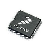
MCF51EM256CLL Freescale Semiconductor, MCF51EM256CLL Datasheet - Page 98

MCF51EM256CLL
Manufacturer Part Number
MCF51EM256CLL
Description
IC MCU 32BIT 256KB FLASH 100LQFP
Manufacturer
Freescale Semiconductor
Series
MCF51EMr
Datasheets
1.MCF51EM128CLL.pdf
(2 pages)
2.MCF51EM128CLL.pdf
(54 pages)
3.MCF51EM128CLL.pdf
(636 pages)
Specifications of MCF51EM256CLL
Core Processor
Coldfire V1
Core Size
32-Bit
Speed
50MHz
Connectivity
I²C, SCI, SPI
Peripherals
LCD, LVD, PWM, WDT
Number Of I /o
63
Program Memory Size
256KB (256K x 8)
Program Memory Type
FLASH
Ram Size
16K x 8
Voltage - Supply (vcc/vdd)
1.8 V ~ 3.6 V
Data Converters
A/D 16x12b
Oscillator Type
External
Operating Temperature
-40°C ~ 85°C
Package / Case
100-LQFP
Processor Series
MCF51EM
Core
ColdFire V1
Data Bus Width
32 bit
Data Ram Size
16 KB
Interface Type
RS-232, LIN
Maximum Clock Frequency
50 MHz
Number Of Timers
3
Operating Supply Voltage
1.8 V to 3.6 V
Maximum Operating Temperature
+ 85 C
Mounting Style
SMD/SMT
3rd Party Development Tools
JLINK-CF-BDM26, EWCF
Development Tools By Supplier
DEMOEM
Minimum Operating Temperature
- 40 C
Lead Free Status / RoHS Status
Lead free / RoHS Compliant
Eeprom Size
-
Lead Free Status / Rohs Status
Lead free / RoHS Compliant
Available stocks
Company
Part Number
Manufacturer
Quantity
Price
Company:
Part Number:
MCF51EM256CLL
Manufacturer:
FREESCALE
Quantity:
110
Company:
Part Number:
MCF51EM256CLL
Manufacturer:
Freescale Semiconductor
Quantity:
10 000
- Current page: 98 of 636
- Download datasheet (11Mb)
Memory
3.4.5.3
The burst program operation will program previously erased data in the flash memory using an embedded
algorithm.
While burst programming, two internal data registers operate as a buffer and a register (2-stage FIFO) so
that a second burst programming command along with the necessary data can be stored to the buffers while
the first burst programming command is still in progress. This pipelined operation allows a time
optimization when programming more than one consecutive address on a specific row in the flash array as
the high voltage generation can be kept active in between two programming commands.
An example flow to execute the burst program operation is shown in
command write sequence is as follows:
The burst program procedure can be used to program the entire flash memory even while crossing row
boundaries within the flash array. If data to be burst programmed falls within a protected area of the flash
array, the FPVIOL flag in the FxSTAT register will set and the burst program command will not launch.
Once the burst program command has successfully launched, the FCCF flag in the FxSTAT register will
set after the burst program operation has completed unless a new burst program command write sequence
has been buffered. By executing a new burst program command write sequence on sequential addresses
after the FCBEF flag in the FxSTAT register has been set, greater than 50% faster programming time for
the entire flash array can be effectively achieved when compared to using the basic program command.
3-42
1. Write to an aligned flash block address to start the command write sequence for the burst program
2. Write the program burst command, 0x25, to the FxCMD register.
3. Clear the FCBEF flag in the FxSTAT register by writing a 1 to FCBEF to launch the program burst
4. After the FCBEF flag in the FxSTAT register returns to a 1, repeat steps 1 through 3. The address
command. The data written will be programmed to the address written.
command.
written is ignored but is incremented internally.
Burst Program Command
MCF51EM256 Series ColdFire Integrated Microcontroller Reference Manual, Rev. 8
Figure
3-12. The burst program
Freescale Semiconductor
Related parts for MCF51EM256CLL
Image
Part Number
Description
Manufacturer
Datasheet
Request
R

Part Number:
Description:
BOARD DEMO HARDWARE ONLY
Manufacturer:
Freescale Semiconductor
Datasheet:

Part Number:
Description:
IC MCU 32BIT 128KB FLASH 100LQFP
Manufacturer:
Freescale Semiconductor
Datasheet:

Part Number:
Description:
IC MCU 32BIT 128KB FLASH 80LQFP
Manufacturer:
Freescale Semiconductor
Datasheet:

Part Number:
Description:
IC MCU 32BIT 256KB FLASH 80LQFP
Manufacturer:
Freescale Semiconductor
Datasheet:
Part Number:
Description:
Manufacturer:
Freescale Semiconductor, Inc
Datasheet:
Part Number:
Description:
Manufacturer:
Freescale Semiconductor, Inc
Datasheet:
Part Number:
Description:
Manufacturer:
Freescale Semiconductor, Inc
Datasheet:
Part Number:
Description:
Manufacturer:
Freescale Semiconductor, Inc
Datasheet:
Part Number:
Description:
Manufacturer:
Freescale Semiconductor, Inc
Datasheet:
Part Number:
Description:
Manufacturer:
Freescale Semiconductor, Inc
Datasheet:
Part Number:
Description:
Manufacturer:
Freescale Semiconductor, Inc
Datasheet:
Part Number:
Description:
Manufacturer:
Freescale Semiconductor, Inc
Datasheet:
Part Number:
Description:
Manufacturer:
Freescale Semiconductor, Inc
Datasheet:
Part Number:
Description:
Manufacturer:
Freescale Semiconductor, Inc
Datasheet:


