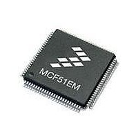
MCF51EM256CLL Freescale Semiconductor, MCF51EM256CLL Datasheet - Page 197

MCF51EM256CLL
Manufacturer Part Number
MCF51EM256CLL
Description
IC MCU 32BIT 256KB FLASH 100LQFP
Manufacturer
Freescale Semiconductor
Series
MCF51EMr
Datasheets
1.MCF51EM128CLL.pdf
(2 pages)
2.MCF51EM128CLL.pdf
(54 pages)
3.MCF51EM128CLL.pdf
(636 pages)
Specifications of MCF51EM256CLL
Core Processor
Coldfire V1
Core Size
32-Bit
Speed
50MHz
Connectivity
I²C, SCI, SPI
Peripherals
LCD, LVD, PWM, WDT
Number Of I /o
63
Program Memory Size
256KB (256K x 8)
Program Memory Type
FLASH
Ram Size
16K x 8
Voltage - Supply (vcc/vdd)
1.8 V ~ 3.6 V
Data Converters
A/D 16x12b
Oscillator Type
External
Operating Temperature
-40°C ~ 85°C
Package / Case
100-LQFP
Processor Series
MCF51EM
Core
ColdFire V1
Data Bus Width
32 bit
Data Ram Size
16 KB
Interface Type
RS-232, LIN
Maximum Clock Frequency
50 MHz
Number Of Timers
3
Operating Supply Voltage
1.8 V to 3.6 V
Maximum Operating Temperature
+ 85 C
Mounting Style
SMD/SMT
3rd Party Development Tools
JLINK-CF-BDM26, EWCF
Development Tools By Supplier
DEMOEM
Minimum Operating Temperature
- 40 C
Lead Free Status / RoHS Status
Lead free / RoHS Compliant
Eeprom Size
-
Lead Free Status / Rohs Status
Lead free / RoHS Compliant
Available stocks
Company
Part Number
Manufacturer
Quantity
Price
Company:
Part Number:
MCF51EM256CLL
Manufacturer:
FREESCALE
Quantity:
110
Company:
Part Number:
MCF51EM256CLL
Manufacturer:
Freescale Semiconductor
Quantity:
10 000
- Current page: 197 of 636
- Download datasheet (11Mb)
8.2.3
This ColdFire architecture supports two independent stack pointer (A7) registers—the supervisor stack
pointer (SSP) and the user stack pointer (USP). The hardware implementation of these two
program-visible 32-bit registers does not identify one as the SSP and the other as the USP. Instead, the
hardware uses one 32-bit register as the active A7 and the other as OTHER_A7. Thus, the register contents
are a function of the processor operation mode, as shown in the following:
if SR[S] = 1
The BDM programming model supports direct reads and writes to A7 and OTHER_A7. It is the
responsibility of the external development system to determine, based on the setting of SR[S], the mapping
of A7 and OTHER_A7 to the two program-visible definitions (SSP and USP).
To support dual stack pointers, the following two supervisor instructions are included in the ColdFire
instruction set architecture to load/store the USP:
These instructions are described in the ColdFire Family Programmer’s Reference Manual. All other
instruction references to the stack pointer, explicit or implicit, access the active A7 register.
8.2.4
The CCR is the LSB of the processor status register (SR). Bits 4–0 act as indicator flags for results
generated by processor operations. The extend bit (X) is also an input operand during multiprecision
arithmetic computations. The CCR register must be explicitly loaded after reset and before any compare
(CMP), Bcc, or Scc instructions are executed.
Freescale Semiconductor
move.l Ay,USP;move to USP
move.l USP,Ax;move from USP
Reset – – – – – – – – – – – – – – – – – – – – – – – – – – – – – – – –
BDM: Load: 0x6F (A7)
then
else
W
R
Supervisor/User Stack Pointers (A7 and OTHER_A7)
Condition Code Register (CCR)
Store: 0x4F (A7)
Load: 0xE0 (OTHER_A7)
Store: 0xC0 (OTHER_A7)
31 30 29 28 27 26 25 24 23 22 21 20 19 18 17 16 15 14 13 12 11 10 9
The USP must be initialized using the
entry into user mode.
The SSP is loaded during reset exception processing with the contents of
location 0x(00)00_0000.
MCF51EM256 Series ColdFire Integrated Microcontroller Reference Manual, Rev. 8
A7 = Supervisor Stack Pointer
OTHER_A7 = User Stack Pointer
A7 = User Stack Pointer
OTHER_A7 = Supervisor Stack Pointer
Figure 8-4. Stack Pointer Registers (A7 and OTHER_A7)
NOTE
move.l Ay,USP
Address
OTHER_A7: Supervisor or BDM read/write
instruction before any
Access: A7: User or BDM read/write
8
7
6
5
4
3
2
ColdFire Core
1
0
8-5
Related parts for MCF51EM256CLL
Image
Part Number
Description
Manufacturer
Datasheet
Request
R

Part Number:
Description:
BOARD DEMO HARDWARE ONLY
Manufacturer:
Freescale Semiconductor
Datasheet:

Part Number:
Description:
IC MCU 32BIT 128KB FLASH 100LQFP
Manufacturer:
Freescale Semiconductor
Datasheet:

Part Number:
Description:
IC MCU 32BIT 128KB FLASH 80LQFP
Manufacturer:
Freescale Semiconductor
Datasheet:

Part Number:
Description:
IC MCU 32BIT 256KB FLASH 80LQFP
Manufacturer:
Freescale Semiconductor
Datasheet:
Part Number:
Description:
Manufacturer:
Freescale Semiconductor, Inc
Datasheet:
Part Number:
Description:
Manufacturer:
Freescale Semiconductor, Inc
Datasheet:
Part Number:
Description:
Manufacturer:
Freescale Semiconductor, Inc
Datasheet:
Part Number:
Description:
Manufacturer:
Freescale Semiconductor, Inc
Datasheet:
Part Number:
Description:
Manufacturer:
Freescale Semiconductor, Inc
Datasheet:
Part Number:
Description:
Manufacturer:
Freescale Semiconductor, Inc
Datasheet:
Part Number:
Description:
Manufacturer:
Freescale Semiconductor, Inc
Datasheet:
Part Number:
Description:
Manufacturer:
Freescale Semiconductor, Inc
Datasheet:
Part Number:
Description:
Manufacturer:
Freescale Semiconductor, Inc
Datasheet:
Part Number:
Description:
Manufacturer:
Freescale Semiconductor, Inc
Datasheet:


