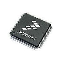
MCF51EM256CLL Freescale Semiconductor, MCF51EM256CLL Datasheet - Page 307

MCF51EM256CLL
Manufacturer Part Number
MCF51EM256CLL
Description
IC MCU 32BIT 256KB FLASH 100LQFP
Manufacturer
Freescale Semiconductor
Series
MCF51EMr
Datasheets
1.MCF51EM128CLL.pdf
(2 pages)
2.MCF51EM128CLL.pdf
(54 pages)
3.MCF51EM128CLL.pdf
(636 pages)
Specifications of MCF51EM256CLL
Core Processor
Coldfire V1
Core Size
32-Bit
Speed
50MHz
Connectivity
I²C, SCI, SPI
Peripherals
LCD, LVD, PWM, WDT
Number Of I /o
63
Program Memory Size
256KB (256K x 8)
Program Memory Type
FLASH
Ram Size
16K x 8
Voltage - Supply (vcc/vdd)
1.8 V ~ 3.6 V
Data Converters
A/D 16x12b
Oscillator Type
External
Operating Temperature
-40°C ~ 85°C
Package / Case
100-LQFP
Processor Series
MCF51EM
Core
ColdFire V1
Data Bus Width
32 bit
Data Ram Size
16 KB
Interface Type
RS-232, LIN
Maximum Clock Frequency
50 MHz
Number Of Timers
3
Operating Supply Voltage
1.8 V to 3.6 V
Maximum Operating Temperature
+ 85 C
Mounting Style
SMD/SMT
3rd Party Development Tools
JLINK-CF-BDM26, EWCF
Development Tools By Supplier
DEMOEM
Minimum Operating Temperature
- 40 C
Lead Free Status / RoHS Status
Lead free / RoHS Compliant
Eeprom Size
-
Lead Free Status / Rohs Status
Lead free / RoHS Compliant
Available stocks
Company
Part Number
Manufacturer
Quantity
Price
Company:
Part Number:
MCF51EM256CLL
Manufacturer:
FREESCALE
Quantity:
110
Company:
Part Number:
MCF51EM256CLL
Manufacturer:
Freescale Semiconductor
Quantity:
10 000
- Current page: 307 of 636
- Download datasheet (11Mb)
13.4.5
The SPI can support data lengths of 8 or 16 bits. The length can be configured with the SPIMODE bit in
the SPIxC2 register.
In 8-bit mode (SPIMODE = 0), the SPI Data Register is comprised of one byte: SPIxDL. The SPI Match
Register is also comprised of only one byte: SPIxML. Reads of SPIxDH and SPIxMH will return zero.
Writes to SPIxDH and SPIxMH will be ignored.
In 16-bit mode (SPIMODE = 1), the SPI Data Register is comprised of two bytes: SPIxDH and SPIxDL.
Reading either byte (SPIxDH or SPIxDL) latches the contents of both bytes into a buffer where they
remain latched until the other byte is read. Writing to either byte (SPIxDH or SPIxDL) latches the value
into a buffer. When both bytes have been written, they are transferred as a coherent 16-bit value into the
transmit data buffer.
In 16-bit mode, the SPI Match Register is also comprised of two bytes: SPIxMH and SPIxML. Reading
either byte (SPIxMH or SPIxML) latches the contents of both bytes into a buffer where they remain latched
until the other byte is read. Writing to either byte (SPIxMH or SPIxML) latches the value into a buffer.
When both bytes have been written, they are transferred as a coherent 16-bit value into the transmit data
buffer.
Any switching between 8- and 16-bit data transmission length (controlled by SPIMODE bit) in master
mode will abort a transmission in progress, force the SPI system into idle state, and reset all status bits in
the SPIxS register. To initiate a transfer after writing to SPIMODE, the SPIxS register must be read with
SPTEF = 1, and data must be written to SPIxDH:SPIxDL in 16-bit mode (SPIMODE = 1) or SPIxDL in
8-bit mode (SPIMODE = 0).
In slave mode, user software should write to SPIMODE only once to prevent corrupting a transmission in
progress.
13.4.6
To accommodate a wide variety of synchronous serial peripherals from different manufacturers, the SPI
system has a clock polarity (CPOL) bit and a clock phase (CPHA) control bit to select one of four clock
formats for data transfers. CPOL selectively inserts an inverter in series with the clock. CPHA chooses
between two different clock phase relationships between the clock and data.
Figure 13-16
figure, the eight bit times are shown for reference with bit 1 starting at the first SPSCK edge and bit 8
ending one-half SPSCK cycle after the sixteenth SPSCK edge. The MSB first and LSB first lines show the
order of SPI data bits depending on the setting in LSBFE. Both variations of SPSCK polarity are shown,
but only one of these waveforms applies for a specific transfer, depending on the value in CPOL. The
SAMPLE IN waveform applies to the MOSI input of a slave or the MISO input of a master. The MOSI
waveform applies to the MOSI output pin from a master and the MISO waveform applies to the MISO
output from a slave. The SS OUT waveform applies to the slave select output from a master (provided
Freescale Semiconductor
Data Transmission Length
SPI Clock Formats
shows the clock formats when SPIMODE = 0 (8-bit mode) and CPHA = 1. At the top of the
Data can be lost if the data length is not the same for both master and slave
devices.
MCF51EM256 Series ColdFire Integrated Microcontroller Reference Manual, Rev. 8
NOTE
16-Bit Serial Peripheral Interface (SPI16)
13-21
Related parts for MCF51EM256CLL
Image
Part Number
Description
Manufacturer
Datasheet
Request
R

Part Number:
Description:
BOARD DEMO HARDWARE ONLY
Manufacturer:
Freescale Semiconductor
Datasheet:

Part Number:
Description:
IC MCU 32BIT 128KB FLASH 100LQFP
Manufacturer:
Freescale Semiconductor
Datasheet:

Part Number:
Description:
IC MCU 32BIT 128KB FLASH 80LQFP
Manufacturer:
Freescale Semiconductor
Datasheet:

Part Number:
Description:
IC MCU 32BIT 256KB FLASH 80LQFP
Manufacturer:
Freescale Semiconductor
Datasheet:
Part Number:
Description:
Manufacturer:
Freescale Semiconductor, Inc
Datasheet:
Part Number:
Description:
Manufacturer:
Freescale Semiconductor, Inc
Datasheet:
Part Number:
Description:
Manufacturer:
Freescale Semiconductor, Inc
Datasheet:
Part Number:
Description:
Manufacturer:
Freescale Semiconductor, Inc
Datasheet:
Part Number:
Description:
Manufacturer:
Freescale Semiconductor, Inc
Datasheet:
Part Number:
Description:
Manufacturer:
Freescale Semiconductor, Inc
Datasheet:
Part Number:
Description:
Manufacturer:
Freescale Semiconductor, Inc
Datasheet:
Part Number:
Description:
Manufacturer:
Freescale Semiconductor, Inc
Datasheet:
Part Number:
Description:
Manufacturer:
Freescale Semiconductor, Inc
Datasheet:
Part Number:
Description:
Manufacturer:
Freescale Semiconductor, Inc
Datasheet:


