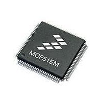
MCF51EM256CLL Freescale Semiconductor, MCF51EM256CLL Datasheet - Page 581

MCF51EM256CLL
Manufacturer Part Number
MCF51EM256CLL
Description
IC MCU 32BIT 256KB FLASH 100LQFP
Manufacturer
Freescale Semiconductor
Series
MCF51EMr
Datasheets
1.MCF51EM128CLL.pdf
(2 pages)
2.MCF51EM128CLL.pdf
(54 pages)
3.MCF51EM128CLL.pdf
(636 pages)
Specifications of MCF51EM256CLL
Core Processor
Coldfire V1
Core Size
32-Bit
Speed
50MHz
Connectivity
I²C, SCI, SPI
Peripherals
LCD, LVD, PWM, WDT
Number Of I /o
63
Program Memory Size
256KB (256K x 8)
Program Memory Type
FLASH
Ram Size
16K x 8
Voltage - Supply (vcc/vdd)
1.8 V ~ 3.6 V
Data Converters
A/D 16x12b
Oscillator Type
External
Operating Temperature
-40°C ~ 85°C
Package / Case
100-LQFP
Processor Series
MCF51EM
Core
ColdFire V1
Data Bus Width
32 bit
Data Ram Size
16 KB
Interface Type
RS-232, LIN
Maximum Clock Frequency
50 MHz
Number Of Timers
3
Operating Supply Voltage
1.8 V to 3.6 V
Maximum Operating Temperature
+ 85 C
Mounting Style
SMD/SMT
3rd Party Development Tools
JLINK-CF-BDM26, EWCF
Development Tools By Supplier
DEMOEM
Minimum Operating Temperature
- 40 C
Lead Free Status / RoHS Status
Lead free / RoHS Compliant
Eeprom Size
-
Lead Free Status / Rohs Status
Lead free / RoHS Compliant
Available stocks
Company
Part Number
Manufacturer
Quantity
Price
Company:
Part Number:
MCF51EM256CLL
Manufacturer:
FREESCALE
Quantity:
110
Company:
Part Number:
MCF51EM256CLL
Manufacturer:
Freescale Semiconductor
Quantity:
10 000
- Current page: 581 of 636
- Download datasheet (11Mb)
26.3.5
BAAR defines the address space for memory-referencing BDM commands. BAAR[R, SZ] are loaded
directly from the BDM command, while the lower five bits can be programmed from the external
Freescale Semiconductor
BFCDIV8
BFCDIV
29–24
Reset
Reset
Field
23–0
DRc: 0x03 (CSR3)
31
30
WDEBUG Instruction No operation during the core’s execution of a WDEBUG instruction
W
W
R
R
WRITE_DREG
READ_DREG
31
15
0
0
0
0
Method
Reserved, must be cleared.
BDM flash clock divide by 8.
0 Input to the flash clock divider is the bus clock
1 Input to the flash clock divider is the bus clock divided by 8
BDM flash clock divider. The BFCDIV8 and BFCDIV fields specify the frequency of the internal flash clock when
performing a mass erase operation initiated by setting XCSR[ERASE]. These fields must be loaded with the
appropriate values prior to the setting of XCSR[ERASE] to initiate a mass erase operation in the flash memory.
This field divides the bus clock (or the bus clock divided by 8 if BFCDIV8 is set) by the value defined by the
BFCDIV plus one. The resulting frequency of the internal flash clock must fall within the range of 150–200 kHz for
proper flash operations. Program/erase timing pulses are one cycle of this internal flash clock, which corresponds
to a range of 5–6.7 μs. The automated programming logic uses an integer number of these pulses to complete
an erase or program operation.
where f
Reserved for future use by the debug module, must be cleared.
BDM Address Attribute Register (BAAR)
DIV8
BFC
MCF51EM256 Series ColdFire Integrated Microcontroller Reference Manual, Rev. 8
30
14
0
0
0
if BFCDIV8 = 0, then f
if BFCDIV8 = 1, then f
FCLK
is the frequency of the flash clock and f
29
13
0
0
0
Reads CSR3[31
Writes CSR3[23
Figure 26-6. Configuration/Status Register 3 (CSR3)
Table 26-10. CSR3 Reference Summary (continued)
28
12
0
0
0
Table 26-11. CSR3 Field Descriptions
27
11
0
0
0
BFCDIV
FCLK
FCLK
–
–
= f
= f
0] from the BDM interface. Classified as a non-intrusive BDM command.
0] from the BDM interface. Classified as a non-intrusive BDM command.
26
10
0
0
0
Bus
Bus
÷ (BFCDIV + 1)
÷ (8 × (BFCDIV + 1)
25
0
9
0
0
24
Description
0
8
0
0
Reference Details
Bus
is the frequency of the bus clock.
23
0
0
0
0
7
22
0
0
0
0
6
21
0
0
0
0
5
Version 1 ColdFire Debug (CF1_DEBUG)
20
0
0
0
0
4
Access: Supervisor write-only
19
0
0
0
0
3
18
0
0
0
0
2
BDM read/write
17
0
0
0
0
1
26-17
16
0
0
0
0
0
Related parts for MCF51EM256CLL
Image
Part Number
Description
Manufacturer
Datasheet
Request
R

Part Number:
Description:
BOARD DEMO HARDWARE ONLY
Manufacturer:
Freescale Semiconductor
Datasheet:

Part Number:
Description:
IC MCU 32BIT 128KB FLASH 100LQFP
Manufacturer:
Freescale Semiconductor
Datasheet:

Part Number:
Description:
IC MCU 32BIT 128KB FLASH 80LQFP
Manufacturer:
Freescale Semiconductor
Datasheet:

Part Number:
Description:
IC MCU 32BIT 256KB FLASH 80LQFP
Manufacturer:
Freescale Semiconductor
Datasheet:
Part Number:
Description:
Manufacturer:
Freescale Semiconductor, Inc
Datasheet:
Part Number:
Description:
Manufacturer:
Freescale Semiconductor, Inc
Datasheet:
Part Number:
Description:
Manufacturer:
Freescale Semiconductor, Inc
Datasheet:
Part Number:
Description:
Manufacturer:
Freescale Semiconductor, Inc
Datasheet:
Part Number:
Description:
Manufacturer:
Freescale Semiconductor, Inc
Datasheet:
Part Number:
Description:
Manufacturer:
Freescale Semiconductor, Inc
Datasheet:
Part Number:
Description:
Manufacturer:
Freescale Semiconductor, Inc
Datasheet:
Part Number:
Description:
Manufacturer:
Freescale Semiconductor, Inc
Datasheet:
Part Number:
Description:
Manufacturer:
Freescale Semiconductor, Inc
Datasheet:
Part Number:
Description:
Manufacturer:
Freescale Semiconductor, Inc
Datasheet:


