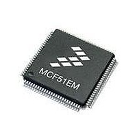
MCF51EM256CLL Freescale Semiconductor, MCF51EM256CLL Datasheet - Page 151

MCF51EM256CLL
Manufacturer Part Number
MCF51EM256CLL
Description
IC MCU 32BIT 256KB FLASH 100LQFP
Manufacturer
Freescale Semiconductor
Series
MCF51EMr
Datasheets
1.MCF51EM128CLL.pdf
(2 pages)
2.MCF51EM128CLL.pdf
(54 pages)
3.MCF51EM128CLL.pdf
(636 pages)
Specifications of MCF51EM256CLL
Core Processor
Coldfire V1
Core Size
32-Bit
Speed
50MHz
Connectivity
I²C, SCI, SPI
Peripherals
LCD, LVD, PWM, WDT
Number Of I /o
63
Program Memory Size
256KB (256K x 8)
Program Memory Type
FLASH
Ram Size
16K x 8
Voltage - Supply (vcc/vdd)
1.8 V ~ 3.6 V
Data Converters
A/D 16x12b
Oscillator Type
External
Operating Temperature
-40°C ~ 85°C
Package / Case
100-LQFP
Processor Series
MCF51EM
Core
ColdFire V1
Data Bus Width
32 bit
Data Ram Size
16 KB
Interface Type
RS-232, LIN
Maximum Clock Frequency
50 MHz
Number Of Timers
3
Operating Supply Voltage
1.8 V to 3.6 V
Maximum Operating Temperature
+ 85 C
Mounting Style
SMD/SMT
3rd Party Development Tools
JLINK-CF-BDM26, EWCF
Development Tools By Supplier
DEMOEM
Minimum Operating Temperature
- 40 C
Lead Free Status / RoHS Status
Lead free / RoHS Compliant
Eeprom Size
-
Lead Free Status / Rohs Status
Lead free / RoHS Compliant
Available stocks
Company
Part Number
Manufacturer
Quantity
Price
Company:
Part Number:
MCF51EM256CLL
Manufacturer:
FREESCALE
Quantity:
110
Company:
Part Number:
MCF51EM256CLL
Manufacturer:
Freescale Semiconductor
Quantity:
10 000
- Current page: 151 of 636
- Download datasheet (11Mb)
The square-wave output frequency was measured and the relative performance results are presented in
Table
as f MHz. The performance of the BCHG loop operating on a GPIO output is selected as the reference.
5.6.2
In this second example, a 16-bit message is transmitted using three programmable output pins. The output
pins include a serial clock, an active-high chip select, and the serial data bit. The software is configured to
sample the serial data bit at the rising-edge of the clock with the data sent in a most-significant to
least-significant bit order. The resulting 3-bit output is shown in
For this example, the processing of the SPI message is considerably more complex than the generation of
a simple square wave of the previous example. The code snippet used to extract the data bit from the
message and build the required GPIO data register writes is shown in
# subtest: send a 16-bit message via a SPI interface using a RGPIO
Freescale Semiconductor
•
5-11. The relative performance is stated as a fraction of the processor’s operating frequency, defined
A pulse counter is decremented until the appropriate number of square-wave pulses have been
generated.
SET+CLR_LOOP — For this construct, two store instructions are executed: one to set the GPIO
data pin and another to clear it. Single-cycle NOP instructions (the tpf opcode) are included to
maintain the 50% duty cycle of the generated square wave. The pulse counter is decremented until
the appropriate number of square-wave pulse have been generated.
set+clr (+toggle) (1/12) × f MHz
gpio_data
gpio_clk
gpio_cs
Application 2: 16-bit Message Transmission using SPI Protocol
Loop
bchg
The square-wave frequency is measured from rising-edge to rising-edge,
where the output wave has a 50% duty cycle.
MCF51EM256 Series ColdFire Integrated Microcontroller Reference Manual, Rev. 8
(1/24) × f MHz
Frequency
# the SPI protocol uses a 3-bit value: clock, chip-select, data
# the data is centered around the rising-edge of the clock
send_16b_spi_message_rgpio:
Sq-Wave
Peripheral Bus-mapped GPIO
Figure 5-9. GPIO SPI Example Timing Diagram
Table 5-11. Square-Wave Output Performance
align
CPU f = 50 MHz
Frequency @
2.083 MHz
4.167 MHz
15
16
NOTE
14
Relative
Speed
1.00x
2.00x
13
(1/14) × f MHz
(1/8) × f MHz
Frequency
Sq-Wave
Figure
2
Figure
5-9.
CPU f = 50 MHz
Frequency @
RGPIO
3.571 MHz
6.250 MHz
5-10.
1
0
Rapid GPIO (RGPIO)
Relative
Speed
1.71x
3.00x
5-11
Related parts for MCF51EM256CLL
Image
Part Number
Description
Manufacturer
Datasheet
Request
R

Part Number:
Description:
BOARD DEMO HARDWARE ONLY
Manufacturer:
Freescale Semiconductor
Datasheet:

Part Number:
Description:
IC MCU 32BIT 128KB FLASH 100LQFP
Manufacturer:
Freescale Semiconductor
Datasheet:

Part Number:
Description:
IC MCU 32BIT 128KB FLASH 80LQFP
Manufacturer:
Freescale Semiconductor
Datasheet:

Part Number:
Description:
IC MCU 32BIT 256KB FLASH 80LQFP
Manufacturer:
Freescale Semiconductor
Datasheet:
Part Number:
Description:
Manufacturer:
Freescale Semiconductor, Inc
Datasheet:
Part Number:
Description:
Manufacturer:
Freescale Semiconductor, Inc
Datasheet:
Part Number:
Description:
Manufacturer:
Freescale Semiconductor, Inc
Datasheet:
Part Number:
Description:
Manufacturer:
Freescale Semiconductor, Inc
Datasheet:
Part Number:
Description:
Manufacturer:
Freescale Semiconductor, Inc
Datasheet:
Part Number:
Description:
Manufacturer:
Freescale Semiconductor, Inc
Datasheet:
Part Number:
Description:
Manufacturer:
Freescale Semiconductor, Inc
Datasheet:
Part Number:
Description:
Manufacturer:
Freescale Semiconductor, Inc
Datasheet:
Part Number:
Description:
Manufacturer:
Freescale Semiconductor, Inc
Datasheet:
Part Number:
Description:
Manufacturer:
Freescale Semiconductor, Inc
Datasheet:


