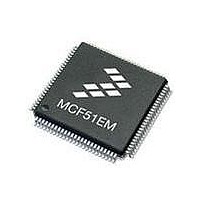
MCF51EM256CLL Freescale Semiconductor, MCF51EM256CLL Datasheet - Page 463

MCF51EM256CLL
Manufacturer Part Number
MCF51EM256CLL
Description
IC MCU 32BIT 256KB FLASH 100LQFP
Manufacturer
Freescale Semiconductor
Series
MCF51EMr
Datasheets
1.MCF51EM128CLL.pdf
(2 pages)
2.MCF51EM128CLL.pdf
(54 pages)
3.MCF51EM128CLL.pdf
(636 pages)
Specifications of MCF51EM256CLL
Core Processor
Coldfire V1
Core Size
32-Bit
Speed
50MHz
Connectivity
I²C, SCI, SPI
Peripherals
LCD, LVD, PWM, WDT
Number Of I /o
63
Program Memory Size
256KB (256K x 8)
Program Memory Type
FLASH
Ram Size
16K x 8
Voltage - Supply (vcc/vdd)
1.8 V ~ 3.6 V
Data Converters
A/D 16x12b
Oscillator Type
External
Operating Temperature
-40°C ~ 85°C
Package / Case
100-LQFP
Processor Series
MCF51EM
Core
ColdFire V1
Data Bus Width
32 bit
Data Ram Size
16 KB
Interface Type
RS-232, LIN
Maximum Clock Frequency
50 MHz
Number Of Timers
3
Operating Supply Voltage
1.8 V to 3.6 V
Maximum Operating Temperature
+ 85 C
Mounting Style
SMD/SMT
3rd Party Development Tools
JLINK-CF-BDM26, EWCF
Development Tools By Supplier
DEMOEM
Minimum Operating Temperature
- 40 C
Lead Free Status / RoHS Status
Lead free / RoHS Compliant
Eeprom Size
-
Lead Free Status / Rohs Status
Lead free / RoHS Compliant
Available stocks
Company
Part Number
Manufacturer
Quantity
Price
Company:
Part Number:
MCF51EM256CLL
Manufacturer:
FREESCALE
Quantity:
110
Company:
Part Number:
MCF51EM256CLL
Manufacturer:
Freescale Semiconductor
Quantity:
10 000
- Current page: 463 of 636
- Download datasheet (11Mb)
21.3.4
V
voltage reference pairs for V
minimum Ref Voltage High (defined in Appendix A) and V
at the same potential as V
V
REFSEL bits.The alternate (V
or internal sources depending on MCU configuration.Consult the module introduction for information on
the Voltage References specific to this MCU.
In some packages, V
reference(s) to the same voltage potential as V
21.3.5
The ADC module supports up to 24 single-ended analog inputs. A single-ended input is selected for
conversion through the ADCHn channel select bits when the DIFFn bit in the ADCSC1n register is low.
21.3.6
The ADC module supports up to four differential analog channel inputs. Each differential analog input is
a pair of external pins (DADPx and DADMx) referenced to each other to provide the most accurate analog
to digital readings. A differential input is selected for conversion through the ADCHn channel select bits
when the DIFFn bit in the ADCSC1n register bit is high.
21.4
These memory-mapped registers control and monitor operation of the ADC:
Freescale Semiconductor
ALTL
REFSL
•
•
•
•
•
•
•
•
•
•
•
•
) and the internal bandgap (V
Status and channel control registers, ADCSC1A:ADCSC1n
Configuration registers, ADCCFG1 and ADCCFG2
Data result registers, ADCRHA:ADCRLA to ADCRHn:ADCRLn
Compare value registers, ADCCV1H, ADCCV1L, ADCCV2H, and ADCCV2L
General status and control registers, ADCSC2 and ADCSC3
Configuration registers, ADCCFG1 and ADCCFG2
Offset Correction Registers, ADCOFSH and ADCOFSL
Plus-input gain registers, ADCPGH and ADCPGL
Minus-input gain registers, ADCMGH and ADCMGL
Plus-side general calibration registers, ADCCLP0, ADCCLP1, ADCCLP2, ADCCLP3H,
ADCCLP3L, ADCCLP4H, ADCCLP4L, ADCCLSP, ADCCLDP
Minus-side general calibration registers, ADCCLM0, ADCCLM1, ADCCLM2, ADCCLM3H,
ADCCLM3L, ADCCLM4H, ADCCLM4L, ADCCLSM, ADCCLDM
Pin enable registers, APCTL1, APCTL2, APCTL3, and APCTL4
is the low reference voltage for the converter.The ADC can be configured to accept one of three
Register Definition
Voltage Reference Select Low (V
Analog Channel Inputs (ADx)
Differential Analog Channel Inputs (DADx)
MCF51EM256 Series ColdFire Integrated Microcontroller Reference Manual, Rev. 8
REFL
is connected in the package to V
SSAD
REFSL
ALTH
. The three pairs are external (V
. Each pair contains a positive reference which must be between the
and V
BGH
and V
ALTL
) voltage reference pair may select additional external pins
SSAD
BGL
). These voltage references are selected using the
.
REFL
SSAD
DDAD
. If externally available, connect the ground
REFH
)
, and a ground reference which must be
and V
Analog-to-Digital Converter (S08ADC16)
REFL
), alternate (V
ALTH
and
21-7
Related parts for MCF51EM256CLL
Image
Part Number
Description
Manufacturer
Datasheet
Request
R

Part Number:
Description:
BOARD DEMO HARDWARE ONLY
Manufacturer:
Freescale Semiconductor
Datasheet:

Part Number:
Description:
IC MCU 32BIT 128KB FLASH 100LQFP
Manufacturer:
Freescale Semiconductor
Datasheet:

Part Number:
Description:
IC MCU 32BIT 128KB FLASH 80LQFP
Manufacturer:
Freescale Semiconductor
Datasheet:

Part Number:
Description:
IC MCU 32BIT 256KB FLASH 80LQFP
Manufacturer:
Freescale Semiconductor
Datasheet:
Part Number:
Description:
Manufacturer:
Freescale Semiconductor, Inc
Datasheet:
Part Number:
Description:
Manufacturer:
Freescale Semiconductor, Inc
Datasheet:
Part Number:
Description:
Manufacturer:
Freescale Semiconductor, Inc
Datasheet:
Part Number:
Description:
Manufacturer:
Freescale Semiconductor, Inc
Datasheet:
Part Number:
Description:
Manufacturer:
Freescale Semiconductor, Inc
Datasheet:
Part Number:
Description:
Manufacturer:
Freescale Semiconductor, Inc
Datasheet:
Part Number:
Description:
Manufacturer:
Freescale Semiconductor, Inc
Datasheet:
Part Number:
Description:
Manufacturer:
Freescale Semiconductor, Inc
Datasheet:
Part Number:
Description:
Manufacturer:
Freescale Semiconductor, Inc
Datasheet:
Part Number:
Description:
Manufacturer:
Freescale Semiconductor, Inc
Datasheet:


