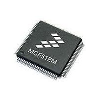
MCF51EM256CLL Freescale Semiconductor, MCF51EM256CLL Datasheet - Page 488

MCF51EM256CLL
Manufacturer Part Number
MCF51EM256CLL
Description
IC MCU 32BIT 256KB FLASH 100LQFP
Manufacturer
Freescale Semiconductor
Series
MCF51EMr
Datasheets
1.MCF51EM128CLL.pdf
(2 pages)
2.MCF51EM128CLL.pdf
(54 pages)
3.MCF51EM128CLL.pdf
(636 pages)
Specifications of MCF51EM256CLL
Core Processor
Coldfire V1
Core Size
32-Bit
Speed
50MHz
Connectivity
I²C, SCI, SPI
Peripherals
LCD, LVD, PWM, WDT
Number Of I /o
63
Program Memory Size
256KB (256K x 8)
Program Memory Type
FLASH
Ram Size
16K x 8
Voltage - Supply (vcc/vdd)
1.8 V ~ 3.6 V
Data Converters
A/D 16x12b
Oscillator Type
External
Operating Temperature
-40°C ~ 85°C
Package / Case
100-LQFP
Processor Series
MCF51EM
Core
ColdFire V1
Data Bus Width
32 bit
Data Ram Size
16 KB
Interface Type
RS-232, LIN
Maximum Clock Frequency
50 MHz
Number Of Timers
3
Operating Supply Voltage
1.8 V to 3.6 V
Maximum Operating Temperature
+ 85 C
Mounting Style
SMD/SMT
3rd Party Development Tools
JLINK-CF-BDM26, EWCF
Development Tools By Supplier
DEMOEM
Minimum Operating Temperature
- 40 C
Lead Free Status / RoHS Status
Lead free / RoHS Compliant
Eeprom Size
-
Lead Free Status / Rohs Status
Lead free / RoHS Compliant
Available stocks
Company
Part Number
Manufacturer
Quantity
Price
Company:
Part Number:
MCF51EM256CLL
Manufacturer:
FREESCALE
Quantity:
110
Company:
Part Number:
MCF51EM256CLL
Manufacturer:
Freescale Semiconductor
Quantity:
10 000
- Current page: 488 of 636
- Download datasheet (11Mb)
Analog-to-Digital Converter (S08ADC16)
21.5.5.6
The following examples use
Table
21.5.5.6.1
A typical configuration for ADC conversion is: 10-bit mode, with the bus clock selected as the input clock
source, the input clock divide-by-1 ratio selected, and a bus frequency of 8 MHz, long sample time
disabled and high speed conversion disabled. The conversion time for a single conversion is calculated by
using
lists the variables of
The resulting conversion time is generated using the parameters listed in
equal to 8 MHz and ADCK equal to 8 MHz, the resulting conversion time is 3.75 us.
21.5.5.6.2
A configuration for long ADC conversion is: 16-bit differential mode, with the bus clock selected as the
input clock source, the input clock divide-by-8 ratio selected, and a bus frequency of 8 MHz, long sample
time enabled and configured for longest adder and high speed conversion disabled. Average enabled for
32 conversions. The conversion time for this conversion is calculated by using
information provided in
Equation
21-32
21-21.
Equation 21-2
21-2.
Conversion Time Examples
The ADCK frequency must be between f
maximum to meet ADC specifications.
Typical conversion time configuration
Long conversion time configuration
MCF51EM256 Series ColdFire Integrated Microcontroller Reference Manual, Rev. 8
Equation
and the information provided in
Table 21-21. High-Speed Conversion Time Adder (HSCAdder)
AverageNum
HSCAdder
SFCAdder
LSTAdder
Variable
Table 21-17
BCT
Equation 21-2
21-2.
Table 21-22. Typical Conversion Time
ADHSC
through
0
1
and the information provided in
Table
5 ADCK cycles + 5 bus clock cycles
Adder (HSCAdder)
NOTE
Conversion Time
0 ADCK cycles
4 ADCK cycles
21-21. The table below list the variables of
High Speed
Table 21-17
20 ADCK cycles
ADCK
Time
1
0
0
minimum and f
through
Table
Table
Table 21-17
ADCK
Equation 21-2
21-24. So, for Bus clock
21-21. The table below
Freescale Semiconductor
through
and the
Related parts for MCF51EM256CLL
Image
Part Number
Description
Manufacturer
Datasheet
Request
R

Part Number:
Description:
BOARD DEMO HARDWARE ONLY
Manufacturer:
Freescale Semiconductor
Datasheet:

Part Number:
Description:
IC MCU 32BIT 128KB FLASH 100LQFP
Manufacturer:
Freescale Semiconductor
Datasheet:

Part Number:
Description:
IC MCU 32BIT 128KB FLASH 80LQFP
Manufacturer:
Freescale Semiconductor
Datasheet:

Part Number:
Description:
IC MCU 32BIT 256KB FLASH 80LQFP
Manufacturer:
Freescale Semiconductor
Datasheet:
Part Number:
Description:
Manufacturer:
Freescale Semiconductor, Inc
Datasheet:
Part Number:
Description:
Manufacturer:
Freescale Semiconductor, Inc
Datasheet:
Part Number:
Description:
Manufacturer:
Freescale Semiconductor, Inc
Datasheet:
Part Number:
Description:
Manufacturer:
Freescale Semiconductor, Inc
Datasheet:
Part Number:
Description:
Manufacturer:
Freescale Semiconductor, Inc
Datasheet:
Part Number:
Description:
Manufacturer:
Freescale Semiconductor, Inc
Datasheet:
Part Number:
Description:
Manufacturer:
Freescale Semiconductor, Inc
Datasheet:
Part Number:
Description:
Manufacturer:
Freescale Semiconductor, Inc
Datasheet:
Part Number:
Description:
Manufacturer:
Freescale Semiconductor, Inc
Datasheet:
Part Number:
Description:
Manufacturer:
Freescale Semiconductor, Inc
Datasheet:


