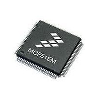
MCF51EM256CLL Freescale Semiconductor, MCF51EM256CLL Datasheet - Page 621

MCF51EM256CLL
Manufacturer Part Number
MCF51EM256CLL
Description
IC MCU 32BIT 256KB FLASH 100LQFP
Manufacturer
Freescale Semiconductor
Series
MCF51EMr
Datasheets
1.MCF51EM128CLL.pdf
(2 pages)
2.MCF51EM128CLL.pdf
(54 pages)
3.MCF51EM128CLL.pdf
(636 pages)
Specifications of MCF51EM256CLL
Core Processor
Coldfire V1
Core Size
32-Bit
Speed
50MHz
Connectivity
I²C, SCI, SPI
Peripherals
LCD, LVD, PWM, WDT
Number Of I /o
63
Program Memory Size
256KB (256K x 8)
Program Memory Type
FLASH
Ram Size
16K x 8
Voltage - Supply (vcc/vdd)
1.8 V ~ 3.6 V
Data Converters
A/D 16x12b
Oscillator Type
External
Operating Temperature
-40°C ~ 85°C
Package / Case
100-LQFP
Processor Series
MCF51EM
Core
ColdFire V1
Data Bus Width
32 bit
Data Ram Size
16 KB
Interface Type
RS-232, LIN
Maximum Clock Frequency
50 MHz
Number Of Timers
3
Operating Supply Voltage
1.8 V to 3.6 V
Maximum Operating Temperature
+ 85 C
Mounting Style
SMD/SMT
3rd Party Development Tools
JLINK-CF-BDM26, EWCF
Development Tools By Supplier
DEMOEM
Minimum Operating Temperature
- 40 C
Lead Free Status / RoHS Status
Lead free / RoHS Compliant
Eeprom Size
-
Lead Free Status / Rohs Status
Lead free / RoHS Compliant
Available stocks
Company
Part Number
Manufacturer
Quantity
Price
Company:
Part Number:
MCF51EM256CLL
Manufacturer:
FREESCALE
Quantity:
110
Company:
Part Number:
MCF51EM256CLL
Manufacturer:
Freescale Semiconductor
Quantity:
10 000
- Current page: 621 of 636
- Download datasheet (11Mb)
The resulting PST/DDATA output stream, with the application program memory image, provides an
instruction-by-instruction dynamic trace of the execution path.
Even with the application of a PST trace buffer, problems associated with the PST bandwidth and
associated fill rate of the buffer remain. Given that there is one (or more) PST entry per instruction, the
PSTB would fill rapidly without some type of data compression.
Consider the following example to illustrate the PST compression algorithm. Most sequential instructions
generate a single PST = 1 value. Without compression, the execution of ten sequential instructions
generates a stream of ten PST = 1 values. With PST compression, the reporting of any PST = 1 value is
delayed so that consecutive PST = 1 values can be accumulated. When a PST ≠ 1 value is reported, the
maximum accumulation count is reached, or a debug data value is captured, a single accumulated PST
value is generated. Returning to the example with compression enabled, the execution of ten sequential
instructions generates a single PST value indicating ten sequential instructions have been executed.
This technique has proven to be effective at significantly reducing the average PST entries per instruction
and PST entries per machine cycle. The application of this compression technique makes the application
of a useful PST trace buffer for the V1 ColdFire core realizable. The resulting 5-bit PST definitions are
shown in
Freescale Semiconductor
0x08–0x0B Indicates the number of data bytes to be loaded into the PST trace buffer. The capturing of peripheral
PST[4:0]
0x00
0x01
0x02
0x03
0x04
0x05
0x06
0x07
Table
26-26.
Continue execution. Many instructions execute in one processor cycle. If an instruction requires more
processor clock cycles, subsequent clock cycles are indicated by driving PST with this encoding.
Begin execution of one instruction. For most instructions, this encoding signals the first processor clock
cycle of an instruction’s execution. Certain change-of-flow opcodes, plus the PULSE and WDDATA
instructions, generate different encodings.
Reserved
Entry into user-mode. Signaled after execution of the instruction that caused the ColdFire processor to
enter user mode.
Begin execution of PULSE and WDDATA instructions. PULSE defines triggers or markers for debug
and/or performance analysis. WDDATA lets the core write any operand (byte, word, or longword)
directly to the DDATA port, independent of debug module configuration. When WDDATA is executed, a
value of 0x04 is signaled on the PST port, followed by the appropriate marker, and then the data transfer
on the DDATA port. The number of captured data bytes depends on the WDDATA operand size.
Begin execution of taken branch or SYNC_PC BDM command. For some opcodes, a branch target
address may be displayed on DDATA depending on the CSR settings. CSR also controls the number of
address bytes displayed, indicated by the PST marker value preceding the DDATA nibble that begins
the data output. This encoding also indicates that the SYNC_PC command has been processed.
Reserved
Begin execution of return from exception (RTE) instruction.
bus data references is controlled by CSR[DDC].
0x08 Begin 1-byte data transfer on DDATA
0x09 Begin 2-byte data transfer on DDATA
0x0A Reserved
0x0B Begin 4-byte data transfer on DDATA
MCF51EM256 Series ColdFire Integrated Microcontroller Reference Manual, Rev. 8
Table 26-26. CF1 Debug Processor Status Encodings
Definition
Version 1 ColdFire Debug (CF1_DEBUG)
26-57
Related parts for MCF51EM256CLL
Image
Part Number
Description
Manufacturer
Datasheet
Request
R

Part Number:
Description:
BOARD DEMO HARDWARE ONLY
Manufacturer:
Freescale Semiconductor
Datasheet:

Part Number:
Description:
IC MCU 32BIT 128KB FLASH 100LQFP
Manufacturer:
Freescale Semiconductor
Datasheet:

Part Number:
Description:
IC MCU 32BIT 128KB FLASH 80LQFP
Manufacturer:
Freescale Semiconductor
Datasheet:

Part Number:
Description:
IC MCU 32BIT 256KB FLASH 80LQFP
Manufacturer:
Freescale Semiconductor
Datasheet:
Part Number:
Description:
Manufacturer:
Freescale Semiconductor, Inc
Datasheet:
Part Number:
Description:
Manufacturer:
Freescale Semiconductor, Inc
Datasheet:
Part Number:
Description:
Manufacturer:
Freescale Semiconductor, Inc
Datasheet:
Part Number:
Description:
Manufacturer:
Freescale Semiconductor, Inc
Datasheet:
Part Number:
Description:
Manufacturer:
Freescale Semiconductor, Inc
Datasheet:
Part Number:
Description:
Manufacturer:
Freescale Semiconductor, Inc
Datasheet:
Part Number:
Description:
Manufacturer:
Freescale Semiconductor, Inc
Datasheet:
Part Number:
Description:
Manufacturer:
Freescale Semiconductor, Inc
Datasheet:
Part Number:
Description:
Manufacturer:
Freescale Semiconductor, Inc
Datasheet:
Part Number:
Description:
Manufacturer:
Freescale Semiconductor, Inc
Datasheet:


