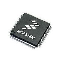
MCF51EM256CLL Freescale Semiconductor, MCF51EM256CLL Datasheet - Page 509

MCF51EM256CLL
Manufacturer Part Number
MCF51EM256CLL
Description
IC MCU 32BIT 256KB FLASH 100LQFP
Manufacturer
Freescale Semiconductor
Series
MCF51EMr
Datasheets
1.MCF51EM128CLL.pdf
(2 pages)
2.MCF51EM128CLL.pdf
(54 pages)
3.MCF51EM128CLL.pdf
(636 pages)
Specifications of MCF51EM256CLL
Core Processor
Coldfire V1
Core Size
32-Bit
Speed
50MHz
Connectivity
I²C, SCI, SPI
Peripherals
LCD, LVD, PWM, WDT
Number Of I /o
63
Program Memory Size
256KB (256K x 8)
Program Memory Type
FLASH
Ram Size
16K x 8
Voltage - Supply (vcc/vdd)
1.8 V ~ 3.6 V
Data Converters
A/D 16x12b
Oscillator Type
External
Operating Temperature
-40°C ~ 85°C
Package / Case
100-LQFP
Processor Series
MCF51EM
Core
ColdFire V1
Data Bus Width
32 bit
Data Ram Size
16 KB
Interface Type
RS-232, LIN
Maximum Clock Frequency
50 MHz
Number Of Timers
3
Operating Supply Voltage
1.8 V to 3.6 V
Maximum Operating Temperature
+ 85 C
Mounting Style
SMD/SMT
3rd Party Development Tools
JLINK-CF-BDM26, EWCF
Development Tools By Supplier
DEMOEM
Minimum Operating Temperature
- 40 C
Lead Free Status / RoHS Status
Lead free / RoHS Compliant
Eeprom Size
-
Lead Free Status / Rohs Status
Lead free / RoHS Compliant
Available stocks
Company
Part Number
Manufacturer
Quantity
Price
Company:
Part Number:
MCF51EM256CLL
Manufacturer:
FREESCALE
Quantity:
110
Company:
Part Number:
MCF51EM256CLL
Manufacturer:
Freescale Semiconductor
Quantity:
10 000
- Current page: 509 of 636
- Download datasheet (11Mb)
22.2.2.6
These registers are used to specify the delay from assertion of TriggerIn to assertion of PreTriggerA and
PreTriggerB out for a given channel. These registers are repeated for each channel present on a given
instance of the PDB. These delays are only applicable if the module is enabled and the output trigger in
question has not been bypassed. In each case, the delay is in terms of PDB source clock cycles.
22.2.3
The PDB contains a single counter whose output is compared against a minimum of three different digital
values. For each channel, DelayA and DelayB determine the time between assertion of the trigger input to
the point at which changes in the trigger output signals are initiated. These times are defined as:
Pre-TriggerA and Pre-TriggerB are used to precondition the ADC blocks two bus clock periods prior to
the actual measurement trigger. The ADC16V1 on MCF51EM256 series MCU contains two sets of control
and result registers, allowing them to operate in a ping-pong fashion, alternating conversions between two
different analog sources (per converter). The Pre-Trigger signals are used to specify which signal will be
sampled next. When PreTriggerA and TriggerA is asserted, the ADC conversion is triggered with set A of
the control and results registers. When PreTriggerB and TriggerB is asserted, the ADC conversion is
triggered with set B of the control and results registers.
Freescale Semiconductor
RESET:
RESET:
W
W
•
•
•
R
R
trigger input to Pre-TriggerA = (prescaler X DelayA) + 2 bus clock cycles
trigger input to Pre-TriggerB = (prescaler X DelayB) + 2 bus clock cycles
Add one additional bus clock cycle to determine the time at which the trigger outputs change.
15
15
0
0
Functional Description
PDB Channel n Delay A & Delay B Registers (PDBCHnDLYA &
PDBCHnDLYB)
MCF51EM256 Series ColdFire Integrated Microcontroller Reference Manual, Rev. 8
14
14
0
0
= Reserved or unused
= Reserved or unused
Figure 22-9. PDB Channel n Delay B Register (PDBCHnDLYB)
Figure 22-8. PDB Channel n Delay A Register (PDBChnDLYA
13
13
0
0
12
12
0
0
11
11
0
0
10
10
0
0
0
0
9
9
DELAY A
DELAY B
0
0
8
8
0
0
7
7
0
0
6
6
0
0
5
5
0
0
4
4
Programmable Delay Block (PDB)
0
0
3
3
0
0
2
2
0
0
1
1
22-9
0
0
0
0
Related parts for MCF51EM256CLL
Image
Part Number
Description
Manufacturer
Datasheet
Request
R

Part Number:
Description:
BOARD DEMO HARDWARE ONLY
Manufacturer:
Freescale Semiconductor
Datasheet:

Part Number:
Description:
IC MCU 32BIT 128KB FLASH 100LQFP
Manufacturer:
Freescale Semiconductor
Datasheet:

Part Number:
Description:
IC MCU 32BIT 128KB FLASH 80LQFP
Manufacturer:
Freescale Semiconductor
Datasheet:

Part Number:
Description:
IC MCU 32BIT 256KB FLASH 80LQFP
Manufacturer:
Freescale Semiconductor
Datasheet:
Part Number:
Description:
Manufacturer:
Freescale Semiconductor, Inc
Datasheet:
Part Number:
Description:
Manufacturer:
Freescale Semiconductor, Inc
Datasheet:
Part Number:
Description:
Manufacturer:
Freescale Semiconductor, Inc
Datasheet:
Part Number:
Description:
Manufacturer:
Freescale Semiconductor, Inc
Datasheet:
Part Number:
Description:
Manufacturer:
Freescale Semiconductor, Inc
Datasheet:
Part Number:
Description:
Manufacturer:
Freescale Semiconductor, Inc
Datasheet:
Part Number:
Description:
Manufacturer:
Freescale Semiconductor, Inc
Datasheet:
Part Number:
Description:
Manufacturer:
Freescale Semiconductor, Inc
Datasheet:
Part Number:
Description:
Manufacturer:
Freescale Semiconductor, Inc
Datasheet:
Part Number:
Description:
Manufacturer:
Freescale Semiconductor, Inc
Datasheet:


