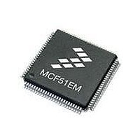
MCF51EM256CLL Freescale Semiconductor, MCF51EM256CLL Datasheet - Page 92

MCF51EM256CLL
Manufacturer Part Number
MCF51EM256CLL
Description
IC MCU 32BIT 256KB FLASH 100LQFP
Manufacturer
Freescale Semiconductor
Series
MCF51EMr
Datasheets
1.MCF51EM128CLL.pdf
(2 pages)
2.MCF51EM128CLL.pdf
(54 pages)
3.MCF51EM128CLL.pdf
(636 pages)
Specifications of MCF51EM256CLL
Core Processor
Coldfire V1
Core Size
32-Bit
Speed
50MHz
Connectivity
I²C, SCI, SPI
Peripherals
LCD, LVD, PWM, WDT
Number Of I /o
63
Program Memory Size
256KB (256K x 8)
Program Memory Type
FLASH
Ram Size
16K x 8
Voltage - Supply (vcc/vdd)
1.8 V ~ 3.6 V
Data Converters
A/D 16x12b
Oscillator Type
External
Operating Temperature
-40°C ~ 85°C
Package / Case
100-LQFP
Processor Series
MCF51EM
Core
ColdFire V1
Data Bus Width
32 bit
Data Ram Size
16 KB
Interface Type
RS-232, LIN
Maximum Clock Frequency
50 MHz
Number Of Timers
3
Operating Supply Voltage
1.8 V to 3.6 V
Maximum Operating Temperature
+ 85 C
Mounting Style
SMD/SMT
3rd Party Development Tools
JLINK-CF-BDM26, EWCF
Development Tools By Supplier
DEMOEM
Minimum Operating Temperature
- 40 C
Lead Free Status / RoHS Status
Lead free / RoHS Compliant
Eeprom Size
-
Lead Free Status / Rohs Status
Lead free / RoHS Compliant
Available stocks
Company
Part Number
Manufacturer
Quantity
Price
Company:
Part Number:
MCF51EM256CLL
Manufacturer:
FREESCALE
Quantity:
110
Company:
Part Number:
MCF51EM256CLL
Manufacturer:
Freescale Semiconductor
Quantity:
10 000
- Current page: 92 of 636
- Download datasheet (11Mb)
Memory
3.4.4
Flash command operations are used to execute program, erase, and erase verify algorithms described in
this section. The program and erase algorithms are controlled by the flash memory controller whose time
base, FCLK, is derived from the bus clock via a programmable divider.
The next sections describe:
3.4.4.1
Prior to issuing any flash command after a reset, the user is required to write the FxCDIV register to divide
the bus clock down to within the 150 kHz to 200 kHz range.
If we define:
then the FxCDIV[PRDIV8, FDIV] bits must be set as described in
For example, if the bus clock frequency is 25 MHz, FxCDIV[FDIV] must be set to 0x0F (001111) and the
FxCDIV[PRDIV8] bit set to 1. The resulting FCLK frequency is then 195 kHz. In this case, the flash
program and erase algorithm timings are increased over the optimum target by:
3-36
FCMD
Field
1. How to write the FxCDIV register to set FCLK
2. Command write sequences to program, erase, and erase verify operations on the flash memory
3. Valid flash commands
4. Effects resulting from illegal flash command write sequences or aborting flash operations
•
•
6–0
7
FCLK as the clock of the flash timing control block
INT(x) as taking the integer part of x (e.g. INT(4.323) = 4)
Flash Command Operations
Reserved, must be cleared.
Flash Command. Valid flash commands are shown below. Writing any command other than those listed sets
the FACCERR flag in the FxSTAT register.
0x05 Erase verify
0x20 Program
0x25 Burst program
0x40 Sector erase
0x41 Mass erase
Writing the FxCDIV Register
MCF51EM256 Series ColdFire Integrated Microcontroller Reference Manual, Rev. 8
Table 3-13. FxCMD Field Descriptions
(200 – 195) ÷ 200 = 3%
Description
Figure
3-9.
Freescale Semiconductor
Eqn. 3-1
Related parts for MCF51EM256CLL
Image
Part Number
Description
Manufacturer
Datasheet
Request
R

Part Number:
Description:
BOARD DEMO HARDWARE ONLY
Manufacturer:
Freescale Semiconductor
Datasheet:

Part Number:
Description:
IC MCU 32BIT 128KB FLASH 100LQFP
Manufacturer:
Freescale Semiconductor
Datasheet:

Part Number:
Description:
IC MCU 32BIT 128KB FLASH 80LQFP
Manufacturer:
Freescale Semiconductor
Datasheet:

Part Number:
Description:
IC MCU 32BIT 256KB FLASH 80LQFP
Manufacturer:
Freescale Semiconductor
Datasheet:
Part Number:
Description:
Manufacturer:
Freescale Semiconductor, Inc
Datasheet:
Part Number:
Description:
Manufacturer:
Freescale Semiconductor, Inc
Datasheet:
Part Number:
Description:
Manufacturer:
Freescale Semiconductor, Inc
Datasheet:
Part Number:
Description:
Manufacturer:
Freescale Semiconductor, Inc
Datasheet:
Part Number:
Description:
Manufacturer:
Freescale Semiconductor, Inc
Datasheet:
Part Number:
Description:
Manufacturer:
Freescale Semiconductor, Inc
Datasheet:
Part Number:
Description:
Manufacturer:
Freescale Semiconductor, Inc
Datasheet:
Part Number:
Description:
Manufacturer:
Freescale Semiconductor, Inc
Datasheet:
Part Number:
Description:
Manufacturer:
Freescale Semiconductor, Inc
Datasheet:
Part Number:
Description:
Manufacturer:
Freescale Semiconductor, Inc
Datasheet:


