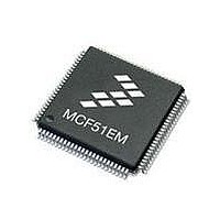
MCF51EM256CLL Freescale Semiconductor, MCF51EM256CLL Datasheet - Page 330

MCF51EM256CLL
Manufacturer Part Number
MCF51EM256CLL
Description
IC MCU 32BIT 256KB FLASH 100LQFP
Manufacturer
Freescale Semiconductor
Series
MCF51EMr
Datasheets
1.MCF51EM128CLL.pdf
(2 pages)
2.MCF51EM128CLL.pdf
(54 pages)
3.MCF51EM128CLL.pdf
(636 pages)
Specifications of MCF51EM256CLL
Core Processor
Coldfire V1
Core Size
32-Bit
Speed
50MHz
Connectivity
I²C, SCI, SPI
Peripherals
LCD, LVD, PWM, WDT
Number Of I /o
63
Program Memory Size
256KB (256K x 8)
Program Memory Type
FLASH
Ram Size
16K x 8
Voltage - Supply (vcc/vdd)
1.8 V ~ 3.6 V
Data Converters
A/D 16x12b
Oscillator Type
External
Operating Temperature
-40°C ~ 85°C
Package / Case
100-LQFP
Processor Series
MCF51EM
Core
ColdFire V1
Data Bus Width
32 bit
Data Ram Size
16 KB
Interface Type
RS-232, LIN
Maximum Clock Frequency
50 MHz
Number Of Timers
3
Operating Supply Voltage
1.8 V to 3.6 V
Maximum Operating Temperature
+ 85 C
Mounting Style
SMD/SMT
3rd Party Development Tools
JLINK-CF-BDM26, EWCF
Development Tools By Supplier
DEMOEM
Minimum Operating Temperature
- 40 C
Lead Free Status / RoHS Status
Lead free / RoHS Compliant
Eeprom Size
-
Lead Free Status / Rohs Status
Lead free / RoHS Compliant
Available stocks
Company
Part Number
Manufacturer
Quantity
Price
Company:
Part Number:
MCF51EM256CLL
Manufacturer:
FREESCALE
Quantity:
110
Company:
Part Number:
MCF51EM256CLL
Manufacturer:
Freescale Semiconductor
Quantity:
10 000
- Current page: 330 of 636
- Download datasheet (11Mb)
Serial Communication Interface (SCI)
1
When using an internal oscillator in a LIN system, it is necessary to raise the break detection threshold one
bit time. Under the worst case timing conditions allowed in LIN, it is possible that a 0x00 data character
can appear to be 10.26 bit times long at a slave running 14% faster than the master. This would trigger
normal break detection circuitry designed to detect a 10-bit break symbol. When the LBKDE bit is set,
framing errors are inhibited and the break detection threshold changes from 10 bits to 11 bits, preventing
false detection of a 0x00 data character as a LIN break symbol.
14.2.6
14-12
Setting RXINV inverts the RxD input for all cases: data bits, start and stop bits, break, and idle.
Reset
LBKDE
TXDIR
Field
Field
RAF
R8
T8
1
0
7
6
5
W
R
SCI Control Register 3 (SCIxC3)
LIN Break Detection Enable. LBKDE selects a longer break character detection length. While LBKDE is set,
framing error (FE) and receive data register full (RDRF) flags are prevented from setting.
0 Break character is detected at length of 10 bit times (11 if M = 1).
1 Break character is detected at length of 11 bit times (12 if M = 1).
Receiver Active Flag. RAF is set when the SCI receiver detects the beginning of a valid start bit, and RAF is
cleared automatically when the receiver detects an idle line. This status flag can be used to check whether an
SCI character is being received before instructing the MCU to go to stop mode.
0 SCI receiver idle waiting for a start bit.
1 SCI receiver active (RxD input not idle).
Ninth Data Bit for Receiver. When the SCI is configured for 9-bit data (M = 1), R8 can be thought of as a ninth
receive data bit to the left of the msb of the buffered data in the SCIxD register. When reading 9-bit data, read
R8 before reading SCIxD because reading SCIxD completes automatic flag clearing sequences that could allow
R8 and SCIxD to be overwritten with new data.
Ninth Data Bit for Transmitter. When the SCI is configured for 9-bit data (M = 1), T8 may be thought of as a ninth
transmit data bit to the left of the msb of the data in the SCIxD register. When writing 9-bit data, the entire 9-bit
value is transferred to the SCI shift register after SCIxD is written so T8 should be written (if it needs to change
from its previous value) before SCIxD is written. If T8 does not need to change in the new value (such as when
it is used to generate mark or space parity), it need not be written each time SCIxD is written.
TxD Pin Direction in Single-Wire Mode. When the SCI is configured for single-wire half-duplex operation
(LOOPS = RSRC = 1), this bit determines the direction of data at the TxD pin.
0 TxD pin is an input in single-wire mode.
1 TxD pin is an output in single-wire mode.
R8
0
7
MCF51EM256 Series ColdFire Integrated Microcontroller Reference Manual, Rev. 8
T8
0
6
Table 14-6. SCIxS2 Field Descriptions (continued)
Figure 14-10. SCI Control Register 3 (SCIxC3)
Table 14-7. SCIxC3 Field Descriptions
TXDIR
0
5
TXINV
0
4
Description
Description
ORIE
3
0
NEIE
0
2
Freescale Semiconductor
FEIE
0
1
PEIE
0
0
Related parts for MCF51EM256CLL
Image
Part Number
Description
Manufacturer
Datasheet
Request
R

Part Number:
Description:
BOARD DEMO HARDWARE ONLY
Manufacturer:
Freescale Semiconductor
Datasheet:

Part Number:
Description:
IC MCU 32BIT 128KB FLASH 100LQFP
Manufacturer:
Freescale Semiconductor
Datasheet:

Part Number:
Description:
IC MCU 32BIT 128KB FLASH 80LQFP
Manufacturer:
Freescale Semiconductor
Datasheet:

Part Number:
Description:
IC MCU 32BIT 256KB FLASH 80LQFP
Manufacturer:
Freescale Semiconductor
Datasheet:
Part Number:
Description:
Manufacturer:
Freescale Semiconductor, Inc
Datasheet:
Part Number:
Description:
Manufacturer:
Freescale Semiconductor, Inc
Datasheet:
Part Number:
Description:
Manufacturer:
Freescale Semiconductor, Inc
Datasheet:
Part Number:
Description:
Manufacturer:
Freescale Semiconductor, Inc
Datasheet:
Part Number:
Description:
Manufacturer:
Freescale Semiconductor, Inc
Datasheet:
Part Number:
Description:
Manufacturer:
Freescale Semiconductor, Inc
Datasheet:
Part Number:
Description:
Manufacturer:
Freescale Semiconductor, Inc
Datasheet:
Part Number:
Description:
Manufacturer:
Freescale Semiconductor, Inc
Datasheet:
Part Number:
Description:
Manufacturer:
Freescale Semiconductor, Inc
Datasheet:
Part Number:
Description:
Manufacturer:
Freescale Semiconductor, Inc
Datasheet:


