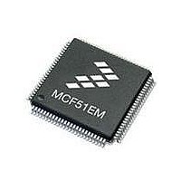
MCF51EM256CLL Freescale Semiconductor, MCF51EM256CLL Datasheet - Page 300

MCF51EM256CLL
Manufacturer Part Number
MCF51EM256CLL
Description
IC MCU 32BIT 256KB FLASH 100LQFP
Manufacturer
Freescale Semiconductor
Series
MCF51EMr
Datasheets
1.MCF51EM128CLL.pdf
(2 pages)
2.MCF51EM128CLL.pdf
(54 pages)
3.MCF51EM128CLL.pdf
(636 pages)
Specifications of MCF51EM256CLL
Core Processor
Coldfire V1
Core Size
32-Bit
Speed
50MHz
Connectivity
I²C, SCI, SPI
Peripherals
LCD, LVD, PWM, WDT
Number Of I /o
63
Program Memory Size
256KB (256K x 8)
Program Memory Type
FLASH
Ram Size
16K x 8
Voltage - Supply (vcc/vdd)
1.8 V ~ 3.6 V
Data Converters
A/D 16x12b
Oscillator Type
External
Operating Temperature
-40°C ~ 85°C
Package / Case
100-LQFP
Processor Series
MCF51EM
Core
ColdFire V1
Data Bus Width
32 bit
Data Ram Size
16 KB
Interface Type
RS-232, LIN
Maximum Clock Frequency
50 MHz
Number Of Timers
3
Operating Supply Voltage
1.8 V to 3.6 V
Maximum Operating Temperature
+ 85 C
Mounting Style
SMD/SMT
3rd Party Development Tools
JLINK-CF-BDM26, EWCF
Development Tools By Supplier
DEMOEM
Minimum Operating Temperature
- 40 C
Lead Free Status / RoHS Status
Lead free / RoHS Compliant
Eeprom Size
-
Lead Free Status / Rohs Status
Lead free / RoHS Compliant
Available stocks
Company
Part Number
Manufacturer
Quantity
Price
Company:
Part Number:
MCF51EM256CLL
Manufacturer:
FREESCALE
Quantity:
110
Company:
Part Number:
MCF51EM256CLL
Manufacturer:
Freescale Semiconductor
Quantity:
10 000
- Current page: 300 of 636
- Download datasheet (11Mb)
16-Bit Serial Peripheral Interface (SPI16)
13.3.7
The SPI Control Register 3 introduces a 64bit FIFO function on both transmit and receive buffers to be
utilised on the SPI. Utilising this FIFO feature allows the SPI to provide high speed transfers of large
amounts of data without consuming large amounts of the CPU bandwidth.
Enabling this FIFO function will effect the behaviour of some of the Read/Write Buffer flags in the SPIxS
register namely:
The SPRF of the SPIxS register will be set when the Receive FIFO is filled and will interrupt the CPU if
the SPIE in the SPIxC1 register is set.
The SPTEF of the SPIxS register will be set when the Transmit FIFO is empty, and will interrupt the CPU
if the SPITIE bit is set in the SPIxC1 register. See SPIxC1 and SPIxS registers.
FIFO mode is enabled by setting the FIFOMODE bit, and provides the SPI with an 8-byte receive FIFO
and an 8-byte transmit FIFO to reduce the amount of CPU interrupts for high speed/high volume data
transfers.
Two interrupt enable bits TNEARIEN and RNFULLIEN provide CPU interrupts based on the
“watermark” feature of the TNEARF and RNFULLF flags of the SPIxS register.
Note: This register has sixread/write control bits. Bits 7 thro’ 6are not implemented and always read 0. Writes have no meaning
13-14
TNEAREF
RNFULLF
Reset
Reset
MARK
MARK
Field
or effect. Write to this register happens only when FIFOMODE bit is 1.
5
4
W
W
R
R
SPI Control Register 3 (SPIxC3) — Enable FIFO Feature
Bit 7
Transmit FIFO Nearly Empty Water Mark - This bit selects the mark after which TNEAREF flag is asserted.
0 TNEAREF is set when Transmit FIFO has16bits or less.
1 TNEAREF is set when Transmit FIFO has 32bits or less.
Receive FIFO Nearly Full Water Mark - This bit selects the mark for which RNFULLF flag is asserted
0 RNFULLF is set when Receive FIFO has 48bits or more
1 RNFULLF is set when Receive FIFO has 32bits or more.
0
0
7
7
MCF51EM256 Series ColdFire Integrated Microcontroller Reference Manual, Rev. 8
= Unimplemented or Reserved
6
0
0
6
6
Figure 13-12. SPI Match Register Low (SPIxML)
Table 13-9. SPIxC3 Register Field Descriptions
Figure 13-13. SPI Status Register (SPIxC3)
TNEAREF
MARK
5
0
0
5
5
RNFULL
MARK
4
0
0
4
4
Description
INTCLR
3
3
0
3
0
TNEARIEN
2
0
0
2
2
RNFULLIEN
Freescale Semiconductor
1
0
0
1
1
FIFOMODE
Bit 0
0
0
0
0
Related parts for MCF51EM256CLL
Image
Part Number
Description
Manufacturer
Datasheet
Request
R

Part Number:
Description:
BOARD DEMO HARDWARE ONLY
Manufacturer:
Freescale Semiconductor
Datasheet:

Part Number:
Description:
IC MCU 32BIT 128KB FLASH 100LQFP
Manufacturer:
Freescale Semiconductor
Datasheet:

Part Number:
Description:
IC MCU 32BIT 128KB FLASH 80LQFP
Manufacturer:
Freescale Semiconductor
Datasheet:

Part Number:
Description:
IC MCU 32BIT 256KB FLASH 80LQFP
Manufacturer:
Freescale Semiconductor
Datasheet:
Part Number:
Description:
Manufacturer:
Freescale Semiconductor, Inc
Datasheet:
Part Number:
Description:
Manufacturer:
Freescale Semiconductor, Inc
Datasheet:
Part Number:
Description:
Manufacturer:
Freescale Semiconductor, Inc
Datasheet:
Part Number:
Description:
Manufacturer:
Freescale Semiconductor, Inc
Datasheet:
Part Number:
Description:
Manufacturer:
Freescale Semiconductor, Inc
Datasheet:
Part Number:
Description:
Manufacturer:
Freescale Semiconductor, Inc
Datasheet:
Part Number:
Description:
Manufacturer:
Freescale Semiconductor, Inc
Datasheet:
Part Number:
Description:
Manufacturer:
Freescale Semiconductor, Inc
Datasheet:
Part Number:
Description:
Manufacturer:
Freescale Semiconductor, Inc
Datasheet:
Part Number:
Description:
Manufacturer:
Freescale Semiconductor, Inc
Datasheet:


