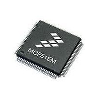
MCF51EM256CLL Freescale Semiconductor, MCF51EM256CLL Datasheet - Page 325

MCF51EM256CLL
Manufacturer Part Number
MCF51EM256CLL
Description
IC MCU 32BIT 256KB FLASH 100LQFP
Manufacturer
Freescale Semiconductor
Series
MCF51EMr
Datasheets
1.MCF51EM128CLL.pdf
(2 pages)
2.MCF51EM128CLL.pdf
(54 pages)
3.MCF51EM128CLL.pdf
(636 pages)
Specifications of MCF51EM256CLL
Core Processor
Coldfire V1
Core Size
32-Bit
Speed
50MHz
Connectivity
I²C, SCI, SPI
Peripherals
LCD, LVD, PWM, WDT
Number Of I /o
63
Program Memory Size
256KB (256K x 8)
Program Memory Type
FLASH
Ram Size
16K x 8
Voltage - Supply (vcc/vdd)
1.8 V ~ 3.6 V
Data Converters
A/D 16x12b
Oscillator Type
External
Operating Temperature
-40°C ~ 85°C
Package / Case
100-LQFP
Processor Series
MCF51EM
Core
ColdFire V1
Data Bus Width
32 bit
Data Ram Size
16 KB
Interface Type
RS-232, LIN
Maximum Clock Frequency
50 MHz
Number Of Timers
3
Operating Supply Voltage
1.8 V to 3.6 V
Maximum Operating Temperature
+ 85 C
Mounting Style
SMD/SMT
3rd Party Development Tools
JLINK-CF-BDM26, EWCF
Development Tools By Supplier
DEMOEM
Minimum Operating Temperature
- 40 C
Lead Free Status / RoHS Status
Lead free / RoHS Compliant
Eeprom Size
-
Lead Free Status / Rohs Status
Lead free / RoHS Compliant
Available stocks
Company
Part Number
Manufacturer
Quantity
Price
Company:
Part Number:
MCF51EM256CLL
Manufacturer:
FREESCALE
Quantity:
110
Company:
Part Number:
MCF51EM256CLL
Manufacturer:
Freescale Semiconductor
Quantity:
10 000
- Current page: 325 of 636
- Download datasheet (11Mb)
14.2.2
This read/write register controls various optional features of the SCI system.
Freescale Semiconductor
SCISWAI
SBR[7:0]
Reset
LOOPS
WAKE
RSRC
Field
Field
7–0
ILT
M
7
6
5
4
3
2
W
R
LOOPS
SCI Control Register 1 (SCIxC1)
Baud Rate Modulo Divisor. These 13 bits in SBR[12:0] are referred to collectively as BR, and they set the modulo
divide rate for the SCI baud rate generator. When BR is cleared, the SCI baud rate generator is disabled to
reduce supply current. When BR is 1 – 8191, the SCI baud rate equals BUSCLK/(16×BR). See also BR bits in
Table
Loop Mode Select. Selects between loop back modes and normal 2-pin full-duplex modes. When LOOPS is set,
the transmitter output is internally connected to the receiver input.
0 Normal operation — RxD and TxD use separate pins.
1 Loop mode or single-wire mode where transmitter outputs are internally connected to receiver input. (See
SCI Stops in Wait Mode
0 SCI clocks continue to run in wait mode so the SCI can be the source of an interrupt that wakes up the CPU.
1 SCI clocks freeze while CPU is in wait mode.
Receiver Source Select. This bit has no meaning or effect unless the LOOPS bit is set to 1. When LOOPS is set,
the receiver input is internally connected to the TxD pin and RSRC determines whether this connection is also
connected to the transmitter output.
0 Provided LOOPS is set, RSRC is cleared, selects internal loop back mode and the SCI does not use the RxD
1 Single-wire SCI mode where the TxD pin is connected to the transmitter output and receiver input.
9-Bit or 8-Bit Mode Select
0 Normal — start + 8 data bits (lsb first) + stop.
1 Receiver and transmitter use 9-bit data characters
Receiver Wakeup Method Select. Refer to
0 Idle-line wakeup.
1 Address-mark wakeup.
Idle Line Type Select. Setting this bit to 1 ensures that the stop bit and logic 1 bits at the end of a character do
not count toward the 10 or 11 bit times of logic high level needed by the idle line detection logic. Refer to
Section 14.3.3.2.1, “Idle-Line
0 Idle character bit count starts after start bit.
1 Idle character bit count starts after stop bit.
0
7
RSRC
pins.
start + 8 data bits (lsb first) + 9th data bit + stop.
MCF51EM256 Series ColdFire Integrated Microcontroller Reference Manual, Rev. 8
14-1.
bit.) RxD pin is not used by SCI.
SCISWAI
0
6
Figure 14-6. SCI Control Register 1 (SCIxC1)
Table 14-2. SCIxBDL Field Descriptions
Table 14-3. SCIxC1 Field Descriptions
RSRC
Wakeup” for more information.
0
5
Section 14.3.3.2, “Receiver Wakeup
M
0
4
Description
Description
WAKE
3
0
ILT
0
2
Serial Communication Interface (SCI)
Operation” for more information.
PE
0
1
PT
0
0
14-7
Related parts for MCF51EM256CLL
Image
Part Number
Description
Manufacturer
Datasheet
Request
R

Part Number:
Description:
BOARD DEMO HARDWARE ONLY
Manufacturer:
Freescale Semiconductor
Datasheet:

Part Number:
Description:
IC MCU 32BIT 128KB FLASH 100LQFP
Manufacturer:
Freescale Semiconductor
Datasheet:

Part Number:
Description:
IC MCU 32BIT 128KB FLASH 80LQFP
Manufacturer:
Freescale Semiconductor
Datasheet:

Part Number:
Description:
IC MCU 32BIT 256KB FLASH 80LQFP
Manufacturer:
Freescale Semiconductor
Datasheet:
Part Number:
Description:
Manufacturer:
Freescale Semiconductor, Inc
Datasheet:
Part Number:
Description:
Manufacturer:
Freescale Semiconductor, Inc
Datasheet:
Part Number:
Description:
Manufacturer:
Freescale Semiconductor, Inc
Datasheet:
Part Number:
Description:
Manufacturer:
Freescale Semiconductor, Inc
Datasheet:
Part Number:
Description:
Manufacturer:
Freescale Semiconductor, Inc
Datasheet:
Part Number:
Description:
Manufacturer:
Freescale Semiconductor, Inc
Datasheet:
Part Number:
Description:
Manufacturer:
Freescale Semiconductor, Inc
Datasheet:
Part Number:
Description:
Manufacturer:
Freescale Semiconductor, Inc
Datasheet:
Part Number:
Description:
Manufacturer:
Freescale Semiconductor, Inc
Datasheet:
Part Number:
Description:
Manufacturer:
Freescale Semiconductor, Inc
Datasheet:


