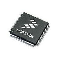
MCF51EM256CLL Freescale Semiconductor, MCF51EM256CLL Datasheet - Page 485

MCF51EM256CLL
Manufacturer Part Number
MCF51EM256CLL
Description
IC MCU 32BIT 256KB FLASH 100LQFP
Manufacturer
Freescale Semiconductor
Series
MCF51EMr
Datasheets
1.MCF51EM128CLL.pdf
(2 pages)
2.MCF51EM128CLL.pdf
(54 pages)
3.MCF51EM128CLL.pdf
(636 pages)
Specifications of MCF51EM256CLL
Core Processor
Coldfire V1
Core Size
32-Bit
Speed
50MHz
Connectivity
I²C, SCI, SPI
Peripherals
LCD, LVD, PWM, WDT
Number Of I /o
63
Program Memory Size
256KB (256K x 8)
Program Memory Type
FLASH
Ram Size
16K x 8
Voltage - Supply (vcc/vdd)
1.8 V ~ 3.6 V
Data Converters
A/D 16x12b
Oscillator Type
External
Operating Temperature
-40°C ~ 85°C
Package / Case
100-LQFP
Processor Series
MCF51EM
Core
ColdFire V1
Data Bus Width
32 bit
Data Ram Size
16 KB
Interface Type
RS-232, LIN
Maximum Clock Frequency
50 MHz
Number Of Timers
3
Operating Supply Voltage
1.8 V to 3.6 V
Maximum Operating Temperature
+ 85 C
Mounting Style
SMD/SMT
3rd Party Development Tools
JLINK-CF-BDM26, EWCF
Development Tools By Supplier
DEMOEM
Minimum Operating Temperature
- 40 C
Lead Free Status / RoHS Status
Lead free / RoHS Compliant
Eeprom Size
-
Lead Free Status / Rohs Status
Lead free / RoHS Compliant
Available stocks
Company
Part Number
Manufacturer
Quantity
Price
Company:
Part Number:
MCF51EM256CLL
Manufacturer:
FREESCALE
Quantity:
110
Company:
Part Number:
MCF51EM256CLL
Manufacturer:
Freescale Semiconductor
Quantity:
10 000
- Current page: 485 of 636
- Download datasheet (11Mb)
21.5.5.3
Any conversion in progress is aborted when:
When a conversion is aborted, the contents of the data registers, ADCRHn and ADCRLn, are not altered.
The data registers continue to be the values transferred after the completion of the last successful
conversion. If the conversion was aborted by a reset or stop2, ADCRHA:ADCRLA and
ADCRHn:ADCRLn return to their reset states.
21.5.5.4
The ADC module remains in its idle state until a conversion is initiated. If ADACK is selected as the
conversion clock source but the asynchronous clock output is disabled (ADACKEN=0), the ADACK
clock generator will also remain in its idle state (disabled) until a conversion is initiated. If the
asynchronous clock output is enabled (ADACKEN=1), it will remain active regardless of the state of the
ADC or the MCU power mode.
Power consumption when the ADC is active can be reduced by setting ADLPC. This results in a lower
maximum value for f
Freescale Semiconductor
•
•
•
•
Writing ADCSC1A while ADCSC1A is actively controlling a conversion aborts the current
conversion. In software trigger mode (ADTRG=0), a write to ADCSC1A initiates a new conversion
(if the ADCHA bits are equal to a value other than all 1s). Writing any of the ADCSC1(B-n)
registers while that specific ADCSC1(B-n) register is actively controlling a conversion aborts the
current conversion.The ADCSC1(B-n) registers are not used for software trigger operation and
therefore writes to the ADCSC1(B-n) registers do not initiate a new conversion.
A write to any ADC register besides the ADCSC1A:ADCSC1n registers occurs. This indicates a
mode of operation change has occurred and the current conversion is therefore invalid.
The MCU is reset or enters stop2 mode.
The MCU enters stop3 mode with ADACK not enabled.
Aborting Conversions
Power Control
If continuous conversions are enabled, the blocking mechanism could result
in the loss of data occurring at specific timepoints. To avoid this issue, the
data must be read in fewer cycles than an ADC conversion time, accounting
for interrupt or software polling loop latency.
If single conversions are enabled, the blocking mechanism could result in
several discarded conversions and excess power consumption. To avoid this
issue, the data registers must not be read after initiating a single conversion
until the conversion completes.
MCF51EM256 Series ColdFire Integrated Microcontroller Reference Manual, Rev. 8
ADCK
(see the electrical specifications).
NOTE
Analog-to-Digital Converter (S08ADC16)
21-29
Related parts for MCF51EM256CLL
Image
Part Number
Description
Manufacturer
Datasheet
Request
R

Part Number:
Description:
BOARD DEMO HARDWARE ONLY
Manufacturer:
Freescale Semiconductor
Datasheet:

Part Number:
Description:
IC MCU 32BIT 128KB FLASH 100LQFP
Manufacturer:
Freescale Semiconductor
Datasheet:

Part Number:
Description:
IC MCU 32BIT 128KB FLASH 80LQFP
Manufacturer:
Freescale Semiconductor
Datasheet:

Part Number:
Description:
IC MCU 32BIT 256KB FLASH 80LQFP
Manufacturer:
Freescale Semiconductor
Datasheet:
Part Number:
Description:
Manufacturer:
Freescale Semiconductor, Inc
Datasheet:
Part Number:
Description:
Manufacturer:
Freescale Semiconductor, Inc
Datasheet:
Part Number:
Description:
Manufacturer:
Freescale Semiconductor, Inc
Datasheet:
Part Number:
Description:
Manufacturer:
Freescale Semiconductor, Inc
Datasheet:
Part Number:
Description:
Manufacturer:
Freescale Semiconductor, Inc
Datasheet:
Part Number:
Description:
Manufacturer:
Freescale Semiconductor, Inc
Datasheet:
Part Number:
Description:
Manufacturer:
Freescale Semiconductor, Inc
Datasheet:
Part Number:
Description:
Manufacturer:
Freescale Semiconductor, Inc
Datasheet:
Part Number:
Description:
Manufacturer:
Freescale Semiconductor, Inc
Datasheet:
Part Number:
Description:
Manufacturer:
Freescale Semiconductor, Inc
Datasheet:


