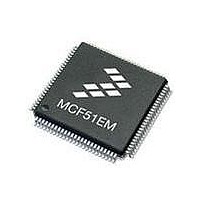
MCF51EM256CLL Freescale Semiconductor, MCF51EM256CLL Datasheet - Page 146

MCF51EM256CLL
Manufacturer Part Number
MCF51EM256CLL
Description
IC MCU 32BIT 256KB FLASH 100LQFP
Manufacturer
Freescale Semiconductor
Series
MCF51EMr
Datasheets
1.MCF51EM128CLL.pdf
(2 pages)
2.MCF51EM128CLL.pdf
(54 pages)
3.MCF51EM128CLL.pdf
(636 pages)
Specifications of MCF51EM256CLL
Core Processor
Coldfire V1
Core Size
32-Bit
Speed
50MHz
Connectivity
I²C, SCI, SPI
Peripherals
LCD, LVD, PWM, WDT
Number Of I /o
63
Program Memory Size
256KB (256K x 8)
Program Memory Type
FLASH
Ram Size
16K x 8
Voltage - Supply (vcc/vdd)
1.8 V ~ 3.6 V
Data Converters
A/D 16x12b
Oscillator Type
External
Operating Temperature
-40°C ~ 85°C
Package / Case
100-LQFP
Processor Series
MCF51EM
Core
ColdFire V1
Data Bus Width
32 bit
Data Ram Size
16 KB
Interface Type
RS-232, LIN
Maximum Clock Frequency
50 MHz
Number Of Timers
3
Operating Supply Voltage
1.8 V to 3.6 V
Maximum Operating Temperature
+ 85 C
Mounting Style
SMD/SMT
3rd Party Development Tools
JLINK-CF-BDM26, EWCF
Development Tools By Supplier
DEMOEM
Minimum Operating Temperature
- 40 C
Lead Free Status / RoHS Status
Lead free / RoHS Compliant
Eeprom Size
-
Lead Free Status / Rohs Status
Lead free / RoHS Compliant
Available stocks
Company
Part Number
Manufacturer
Quantity
Price
Company:
Part Number:
MCF51EM256CLL
Manufacturer:
FREESCALE
Quantity:
110
Company:
Part Number:
MCF51EM256CLL
Manufacturer:
Freescale Semiconductor
Quantity:
10 000
- Current page: 146 of 636
- Download datasheet (11Mb)
Rapid GPIO (RGPIO)
5.3
The RGPIO module provides a compact 16-byte programming model based at a system memory address
of 0x(00)C0_0000 (noted as RGPIO_BASE throughout the chapter). As previously noted, the
programming model views are different between reads and writes as this enables simplified software for
manipulation of the RGPIO pins. Additionally, the programming model can be referenced using any
operand size access (byte, word, longword). Performance is typically maximized using 32-bit accesses.
5.3.1
The read/write RGPIO_DIR register defines whether a properly-enabled RGPIO pin is configured as an
input or output:
5-6
•
•
Address
Address
Offset
Offset
0x0C
0x0A
0x0E
0x0A
0x0E
0x00
0x02
0x04
0x06
0x00
0x02
0x04
0x06
0x08
Setting any bit in RGPIO_DIR configures a properly-enabled RGPIO port pin as an output
Clearing any bit in RGPIO_DIR configures a properly-enabled RGPIO port pin as an input
Memory Map/Register Definition
RGPIO Data Direction (RGPIO_DIR)
Writes to the two-byte fields at RGPIO_BASE + 0x8 and
RGPIO_BASE + 0xC are allowed, but do not affect any program-visible
register within the RGPIO module.
RGPIO Data Direction Register (RGPIO_DIR)
RGPIO Write Data Register (RGPIO_DATA)
RGPIO Pin Enable Register (RGPIO_ENB)
RGPIO Write Data Clear Register (RGPIO_CLR)
RGPIO Write Data Set Register (RGPIO_SET)
RGPIO Write Data Toggle Register (RGPIO_TOG)
MCF51EM256 Series ColdFire Integrated Microcontroller Reference Manual, Rev. 8
RGPIO data direction register (RGPIO_DIR)
RGPIO write data register (RGPIO_DATA)
RGPIO pin enable register (RGPIO_ENB)
RGPIO write data register (RGPIO_DATA)
RGPIO data direction register (RGPIO_DIR)
RGPIO write data register (RGPIO_DATA)
RGPIO data direction register (RGPIO_DIR)
RGPIO write data register (RGPIO_DATA)
Register
Register
Table 5-3. RGPIO Write Memory Map
Table 5-4. RGPIO Read Memory Map
NOTE
Width
Width
(bits)
(bits)
16
16
16
16
16
16
16
16
16
16
16
16
16
16
Access Reset Value
Access Reset Value
W
W
W
W
W
W
R
R
R
R
R
R
R
R
0x0000
0x0000
0x0000
0x0000
0x0000
0x0000
0x0000
0x0000
0x0000
0x0000
0x0000
N/A
N/A
N/A
Freescale Semiconductor
Section/Page
Section/Page
5.3.1/5-6
5.3.2/5-7
5.3.3/5-8
5.3.4/5-8
5.3.5/5-9
5.3.6/5-9
5.3.1/5-6
5.3.2/5-7
5.3.3/5-8
5.3.2/5-7
5.3.1/5-6
5.3.2/5-7
5.3.1/5-6
5.3.2/5-7
Related parts for MCF51EM256CLL
Image
Part Number
Description
Manufacturer
Datasheet
Request
R

Part Number:
Description:
BOARD DEMO HARDWARE ONLY
Manufacturer:
Freescale Semiconductor
Datasheet:

Part Number:
Description:
IC MCU 32BIT 128KB FLASH 100LQFP
Manufacturer:
Freescale Semiconductor
Datasheet:

Part Number:
Description:
IC MCU 32BIT 128KB FLASH 80LQFP
Manufacturer:
Freescale Semiconductor
Datasheet:

Part Number:
Description:
IC MCU 32BIT 256KB FLASH 80LQFP
Manufacturer:
Freescale Semiconductor
Datasheet:
Part Number:
Description:
Manufacturer:
Freescale Semiconductor, Inc
Datasheet:
Part Number:
Description:
Manufacturer:
Freescale Semiconductor, Inc
Datasheet:
Part Number:
Description:
Manufacturer:
Freescale Semiconductor, Inc
Datasheet:
Part Number:
Description:
Manufacturer:
Freescale Semiconductor, Inc
Datasheet:
Part Number:
Description:
Manufacturer:
Freescale Semiconductor, Inc
Datasheet:
Part Number:
Description:
Manufacturer:
Freescale Semiconductor, Inc
Datasheet:
Part Number:
Description:
Manufacturer:
Freescale Semiconductor, Inc
Datasheet:
Part Number:
Description:
Manufacturer:
Freescale Semiconductor, Inc
Datasheet:
Part Number:
Description:
Manufacturer:
Freescale Semiconductor, Inc
Datasheet:
Part Number:
Description:
Manufacturer:
Freescale Semiconductor, Inc
Datasheet:


