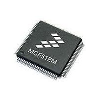
MCF51EM256CLL Freescale Semiconductor, MCF51EM256CLL Datasheet - Page 243

MCF51EM256CLL
Manufacturer Part Number
MCF51EM256CLL
Description
IC MCU 32BIT 256KB FLASH 100LQFP
Manufacturer
Freescale Semiconductor
Series
MCF51EMr
Datasheets
1.MCF51EM128CLL.pdf
(2 pages)
2.MCF51EM128CLL.pdf
(54 pages)
3.MCF51EM128CLL.pdf
(636 pages)
Specifications of MCF51EM256CLL
Core Processor
Coldfire V1
Core Size
32-Bit
Speed
50MHz
Connectivity
I²C, SCI, SPI
Peripherals
LCD, LVD, PWM, WDT
Number Of I /o
63
Program Memory Size
256KB (256K x 8)
Program Memory Type
FLASH
Ram Size
16K x 8
Voltage - Supply (vcc/vdd)
1.8 V ~ 3.6 V
Data Converters
A/D 16x12b
Oscillator Type
External
Operating Temperature
-40°C ~ 85°C
Package / Case
100-LQFP
Processor Series
MCF51EM
Core
ColdFire V1
Data Bus Width
32 bit
Data Ram Size
16 KB
Interface Type
RS-232, LIN
Maximum Clock Frequency
50 MHz
Number Of Timers
3
Operating Supply Voltage
1.8 V to 3.6 V
Maximum Operating Temperature
+ 85 C
Mounting Style
SMD/SMT
3rd Party Development Tools
JLINK-CF-BDM26, EWCF
Development Tools By Supplier
DEMOEM
Minimum Operating Temperature
- 40 C
Lead Free Status / RoHS Status
Lead free / RoHS Compliant
Eeprom Size
-
Lead Free Status / Rohs Status
Lead free / RoHS Compliant
Available stocks
Company
Part Number
Manufacturer
Quantity
Price
Company:
Part Number:
MCF51EM256CLL
Manufacturer:
FREESCALE
Quantity:
110
Company:
Part Number:
MCF51EM256CLL
Manufacturer:
Freescale Semiconductor
Quantity:
10 000
- Current page: 243 of 636
- Download datasheet (11Mb)
10.1.3
The CF1_INTC module does not support any special modes of operation. As a memory-mapped slave
peripheral located on the platform’s slave bus, it responds based strictly on the memory addresses of the
connected bus.
One special behavior of the CF1_INTC deserves mention. When the device enters a wait or stop mode and
certain clocks are disabled, there is an input signal that can be asserted to enable a purely-combinational
logic path for monitoring the assertion of an interrupt request. After a request of unmasked level is
asserted, this combinational logic path asserts an output signal that is sent to the clock generation logic to
re-enable the internal device clocks to exit the low-power mode.
10.2
The CF1_INTC module does not include any external interfaces.
10.3
The CF1_INTC module provides a 64-byte programming model mapped to the upper region of the 16 MB
address space. All the register names are prefixed with INTC_ as an abbreviation for the full module name.
The programming model is referenced using 8-bit accesses. Attempted references to undefined (reserved)
addresses or with a non-supported access type (for example, a write to a read-only register) generate a bus
error termination.
The programming model follows the definition from previous ColdFire interrupt controllers. This
compatibility accounts for the various memory holes in this module’s memory map.
The CF1_INTC module is based at address 0x(FF)FF_FFC0 (referred to as CF1_INTC_BASE throughout
the chapter) and occupies the upper 64 bytes of the peripheral space. The module memory map is shown
in
Freescale Semiconductor
Table
•
•
•
— Exactly matches HCS08 interrupt request priorities
— Up to two requests can be remapped to the highest maskable level + priority
Unique vector number for each interrupt source
— ColdFire vector number = 62 + HCS08 vector number
— Details on IRQ and vector assignments are device-specific
Support for service routine interrupt acknowledge (software IACK) read cycles for improved
system performance
Combinatorial path provides wakeup signal from wait and stop modes
10-3.
External Signal Description
Memory Map/Register Definition
Modes of Operation
MCF51EM256 Series ColdFire Integrated Microcontroller Reference Manual, Rev. 8
Interrupt Controller (CF1_INTC)
10-7
Related parts for MCF51EM256CLL
Image
Part Number
Description
Manufacturer
Datasheet
Request
R

Part Number:
Description:
BOARD DEMO HARDWARE ONLY
Manufacturer:
Freescale Semiconductor
Datasheet:

Part Number:
Description:
IC MCU 32BIT 128KB FLASH 100LQFP
Manufacturer:
Freescale Semiconductor
Datasheet:

Part Number:
Description:
IC MCU 32BIT 128KB FLASH 80LQFP
Manufacturer:
Freescale Semiconductor
Datasheet:

Part Number:
Description:
IC MCU 32BIT 256KB FLASH 80LQFP
Manufacturer:
Freescale Semiconductor
Datasheet:
Part Number:
Description:
Manufacturer:
Freescale Semiconductor, Inc
Datasheet:
Part Number:
Description:
Manufacturer:
Freescale Semiconductor, Inc
Datasheet:
Part Number:
Description:
Manufacturer:
Freescale Semiconductor, Inc
Datasheet:
Part Number:
Description:
Manufacturer:
Freescale Semiconductor, Inc
Datasheet:
Part Number:
Description:
Manufacturer:
Freescale Semiconductor, Inc
Datasheet:
Part Number:
Description:
Manufacturer:
Freescale Semiconductor, Inc
Datasheet:
Part Number:
Description:
Manufacturer:
Freescale Semiconductor, Inc
Datasheet:
Part Number:
Description:
Manufacturer:
Freescale Semiconductor, Inc
Datasheet:
Part Number:
Description:
Manufacturer:
Freescale Semiconductor, Inc
Datasheet:
Part Number:
Description:
Manufacturer:
Freescale Semiconductor, Inc
Datasheet:


