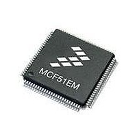
MCF51EM256CLL Freescale Semiconductor, MCF51EM256CLL Datasheet - Page 423

MCF51EM256CLL
Manufacturer Part Number
MCF51EM256CLL
Description
IC MCU 32BIT 256KB FLASH 100LQFP
Manufacturer
Freescale Semiconductor
Series
MCF51EMr
Datasheets
1.MCF51EM128CLL.pdf
(2 pages)
2.MCF51EM128CLL.pdf
(54 pages)
3.MCF51EM128CLL.pdf
(636 pages)
Specifications of MCF51EM256CLL
Core Processor
Coldfire V1
Core Size
32-Bit
Speed
50MHz
Connectivity
I²C, SCI, SPI
Peripherals
LCD, LVD, PWM, WDT
Number Of I /o
63
Program Memory Size
256KB (256K x 8)
Program Memory Type
FLASH
Ram Size
16K x 8
Voltage - Supply (vcc/vdd)
1.8 V ~ 3.6 V
Data Converters
A/D 16x12b
Oscillator Type
External
Operating Temperature
-40°C ~ 85°C
Package / Case
100-LQFP
Processor Series
MCF51EM
Core
ColdFire V1
Data Bus Width
32 bit
Data Ram Size
16 KB
Interface Type
RS-232, LIN
Maximum Clock Frequency
50 MHz
Number Of Timers
3
Operating Supply Voltage
1.8 V to 3.6 V
Maximum Operating Temperature
+ 85 C
Mounting Style
SMD/SMT
3rd Party Development Tools
JLINK-CF-BDM26, EWCF
Development Tools By Supplier
DEMOEM
Minimum Operating Temperature
- 40 C
Lead Free Status / RoHS Status
Lead free / RoHS Compliant
Eeprom Size
-
Lead Free Status / Rohs Status
Lead free / RoHS Compliant
Available stocks
Company
Part Number
Manufacturer
Quantity
Price
Company:
Part Number:
MCF51EM256CLL
Manufacturer:
FREESCALE
Quantity:
110
Company:
Part Number:
MCF51EM256CLL
Manufacturer:
Freescale Semiconductor
Quantity:
10 000
- Current page: 423 of 636
- Download datasheet (11Mb)
Independent Robust Real Time Clock (IRTC)
disabled the compensation logic. If no value is programmed the state machine continues to perform
compensation with the previously programmed values till compensation is disabled by writing zero as the
compensation interval. Figure below shows the block diagram for the compensation block.
Recommendation for Optimal Compensation:
Since the addition and removal of pulses is done in the first second of the compensation interval, the CPU
has the option of finding the compensation factor over a period of time and then calculating the correction
factor per second and enable compensation hardware every second for better accuracy. The 1 Hz clock
generated will have uniform period.
Figure 17-28. Compensation Logic Block Diagram
17.8.2
Write Protection Logic
This logic protects the IRTC registers and Standby RAM from any spurious updates that can happen due
run-away code. The logic is based on a state machine that monitors the values written to WE[1:0] bits of
the IRTC_CTRL register. By default unconditional write access is allowed to these bits only.
To enable write protection, “10” is written on these bits. To disable write protection, the sequence “00 –
01 – 11 – 10” is written onto these bits.
After a power on reset, the write-protect mechanism is disabled, allowing the user code to calibrate the
IRTC clock, set the time in the clock registers, and set the date in the calendar registers. Once calibration
and time & date settings are done, the user code should enable write protection mode. If not, the registers
are put into write protect mode 15 seconds after power on. In case the write protect mode is unlocked to
update registers, then the write protect mode is enabled 2 seconds after unlock if not done by CPU.
Any access made to the register space when write protection is enabled (i.e. registers in locked mode) will
cause the transfer error signal to be asserted.
MCF51EM256 Series ColdFire Integrated Microcontroller Reference Manual, Rev. 8
Freescale Semiconductor
17-39
Related parts for MCF51EM256CLL
Image
Part Number
Description
Manufacturer
Datasheet
Request
R

Part Number:
Description:
BOARD DEMO HARDWARE ONLY
Manufacturer:
Freescale Semiconductor
Datasheet:

Part Number:
Description:
IC MCU 32BIT 128KB FLASH 100LQFP
Manufacturer:
Freescale Semiconductor
Datasheet:

Part Number:
Description:
IC MCU 32BIT 128KB FLASH 80LQFP
Manufacturer:
Freescale Semiconductor
Datasheet:

Part Number:
Description:
IC MCU 32BIT 256KB FLASH 80LQFP
Manufacturer:
Freescale Semiconductor
Datasheet:
Part Number:
Description:
Manufacturer:
Freescale Semiconductor, Inc
Datasheet:
Part Number:
Description:
Manufacturer:
Freescale Semiconductor, Inc
Datasheet:
Part Number:
Description:
Manufacturer:
Freescale Semiconductor, Inc
Datasheet:
Part Number:
Description:
Manufacturer:
Freescale Semiconductor, Inc
Datasheet:
Part Number:
Description:
Manufacturer:
Freescale Semiconductor, Inc
Datasheet:
Part Number:
Description:
Manufacturer:
Freescale Semiconductor, Inc
Datasheet:
Part Number:
Description:
Manufacturer:
Freescale Semiconductor, Inc
Datasheet:
Part Number:
Description:
Manufacturer:
Freescale Semiconductor, Inc
Datasheet:
Part Number:
Description:
Manufacturer:
Freescale Semiconductor, Inc
Datasheet:
Part Number:
Description:
Manufacturer:
Freescale Semiconductor, Inc
Datasheet:


