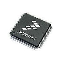
MCF51EM256CLL Freescale Semiconductor, MCF51EM256CLL Datasheet - Page 176

MCF51EM256CLL
Manufacturer Part Number
MCF51EM256CLL
Description
IC MCU 32BIT 256KB FLASH 100LQFP
Manufacturer
Freescale Semiconductor
Series
MCF51EMr
Datasheets
1.MCF51EM128CLL.pdf
(2 pages)
2.MCF51EM128CLL.pdf
(54 pages)
3.MCF51EM128CLL.pdf
(636 pages)
Specifications of MCF51EM256CLL
Core Processor
Coldfire V1
Core Size
32-Bit
Speed
50MHz
Connectivity
I²C, SCI, SPI
Peripherals
LCD, LVD, PWM, WDT
Number Of I /o
63
Program Memory Size
256KB (256K x 8)
Program Memory Type
FLASH
Ram Size
16K x 8
Voltage - Supply (vcc/vdd)
1.8 V ~ 3.6 V
Data Converters
A/D 16x12b
Oscillator Type
External
Operating Temperature
-40°C ~ 85°C
Package / Case
100-LQFP
Processor Series
MCF51EM
Core
ColdFire V1
Data Bus Width
32 bit
Data Ram Size
16 KB
Interface Type
RS-232, LIN
Maximum Clock Frequency
50 MHz
Number Of Timers
3
Operating Supply Voltage
1.8 V to 3.6 V
Maximum Operating Temperature
+ 85 C
Mounting Style
SMD/SMT
3rd Party Development Tools
JLINK-CF-BDM26, EWCF
Development Tools By Supplier
DEMOEM
Minimum Operating Temperature
- 40 C
Lead Free Status / RoHS Status
Lead free / RoHS Compliant
Eeprom Size
-
Lead Free Status / Rohs Status
Lead free / RoHS Compliant
Available stocks
Company
Part Number
Manufacturer
Quantity
Price
Company:
Part Number:
MCF51EM256CLL
Manufacturer:
FREESCALE
Quantity:
110
Company:
Part Number:
MCF51EM256CLL
Manufacturer:
Freescale Semiconductor
Quantity:
10 000
- Current page: 176 of 636
- Download datasheet (11Mb)
Resets, Interrupts, and General System Control
LVWF is cleared by writing a 1 to the SPMSC3[LVWACK] bit. There are two user-selectable trip voltages
for the LVW, one high (V
bit.
7.6
The MCF51EM series microcontroller includes a clock gating system to manage the bus clock sources to
the individual peripherals. Using this system, the user can enable or disable the bus clock to each of the
peripherals at the clock source, eliminating unnecessary clocks to peripherals which are not in use; thereby
reducing the overall run and wait mode currents.
Out of reset, all peripheral clocks will be enabled. For lowest possible run or wait currents, user software
should disable the clock source to any peripheral not in use. The actual clock will be enabled or disabled
immediately following the write to the clock gating control registers (SCGC1, SCGC2, SCGC3, SCGC4).
Any peripheral with a gated clock can not be used unless its clock is enabled. Writing to the registers of a
peripheral with a disabled clock has no effect.
In stop modes, the bus clock is disabled for all gated peripherals, regardless of the settings in the SCGC1,
SCGC2, SCGC3 and SCGC4 registers.
7.7
One 8-bit register in the direct page register space and eight 8-bit registers in the high-page register space
are related to reset and interrupt systems.
Refer to
assignments for all registers. This section refers to registers and control bits only by their names. A
Freescale-provided equate or header file is used to translate these names into the appropriate absolute
addresses.
Some control bits in the SOPT1 and SPMSC2 registers are related to modes of operation. Although brief
descriptions of these bits are provided here, the related functions are discussed in greater detail in
Chapter 6, “Modes of Operation.”
7-10
Section 3.2, “Detailed Register Addresses and Bit
Peripheral Clock Gating
Reset, Interrupt, and System Control Registers and Control Bits
User software should disable the peripheral before disabling the clocks to
the peripheral. When clocks are re-enabled to a peripheral, the peripheral
registers need to be re-initialized by user software.
MCF51EM256 Series ColdFire Integrated Microcontroller Reference Manual, Rev. 8
LVWH
) and one low (V
LVWL
NOTE
). The trip voltage is selected by SPMSC3[LVWV]
Assignments,” for the absolute address
Freescale Semiconductor
Related parts for MCF51EM256CLL
Image
Part Number
Description
Manufacturer
Datasheet
Request
R

Part Number:
Description:
BOARD DEMO HARDWARE ONLY
Manufacturer:
Freescale Semiconductor
Datasheet:

Part Number:
Description:
IC MCU 32BIT 128KB FLASH 100LQFP
Manufacturer:
Freescale Semiconductor
Datasheet:

Part Number:
Description:
IC MCU 32BIT 128KB FLASH 80LQFP
Manufacturer:
Freescale Semiconductor
Datasheet:

Part Number:
Description:
IC MCU 32BIT 256KB FLASH 80LQFP
Manufacturer:
Freescale Semiconductor
Datasheet:
Part Number:
Description:
Manufacturer:
Freescale Semiconductor, Inc
Datasheet:
Part Number:
Description:
Manufacturer:
Freescale Semiconductor, Inc
Datasheet:
Part Number:
Description:
Manufacturer:
Freescale Semiconductor, Inc
Datasheet:
Part Number:
Description:
Manufacturer:
Freescale Semiconductor, Inc
Datasheet:
Part Number:
Description:
Manufacturer:
Freescale Semiconductor, Inc
Datasheet:
Part Number:
Description:
Manufacturer:
Freescale Semiconductor, Inc
Datasheet:
Part Number:
Description:
Manufacturer:
Freescale Semiconductor, Inc
Datasheet:
Part Number:
Description:
Manufacturer:
Freescale Semiconductor, Inc
Datasheet:
Part Number:
Description:
Manufacturer:
Freescale Semiconductor, Inc
Datasheet:
Part Number:
Description:
Manufacturer:
Freescale Semiconductor, Inc
Datasheet:


