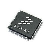
MCF51EM256CLL Freescale Semiconductor, MCF51EM256CLL Datasheet - Page 498

MCF51EM256CLL
Manufacturer Part Number
MCF51EM256CLL
Description
IC MCU 32BIT 256KB FLASH 100LQFP
Manufacturer
Freescale Semiconductor
Series
MCF51EMr
Datasheets
1.MCF51EM128CLL.pdf
(2 pages)
2.MCF51EM128CLL.pdf
(54 pages)
3.MCF51EM128CLL.pdf
(636 pages)
Specifications of MCF51EM256CLL
Core Processor
Coldfire V1
Core Size
32-Bit
Speed
50MHz
Connectivity
I²C, SCI, SPI
Peripherals
LCD, LVD, PWM, WDT
Number Of I /o
63
Program Memory Size
256KB (256K x 8)
Program Memory Type
FLASH
Ram Size
16K x 8
Voltage - Supply (vcc/vdd)
1.8 V ~ 3.6 V
Data Converters
A/D 16x12b
Oscillator Type
External
Operating Temperature
-40°C ~ 85°C
Package / Case
100-LQFP
Processor Series
MCF51EM
Core
ColdFire V1
Data Bus Width
32 bit
Data Ram Size
16 KB
Interface Type
RS-232, LIN
Maximum Clock Frequency
50 MHz
Number Of Timers
3
Operating Supply Voltage
1.8 V to 3.6 V
Maximum Operating Temperature
+ 85 C
Mounting Style
SMD/SMT
3rd Party Development Tools
JLINK-CF-BDM26, EWCF
Development Tools By Supplier
DEMOEM
Minimum Operating Temperature
- 40 C
Lead Free Status / RoHS Status
Lead free / RoHS Compliant
Eeprom Size
-
Lead Free Status / Rohs Status
Lead free / RoHS Compliant
Available stocks
Company
Part Number
Manufacturer
Quantity
Price
Company:
Part Number:
MCF51EM256CLL
Manufacturer:
FREESCALE
Quantity:
110
Company:
Part Number:
MCF51EM256CLL
Manufacturer:
Freescale Semiconductor
Quantity:
10 000
- Current page: 498 of 636
- Download datasheet (11Mb)
Analog-to-Digital Converter (S08ADC16)
21.7.1.3
The external analog inputs are typically shared with digital I/O pins on MCU devices. The pin I/O control
is disabled by setting the appropriate control bit in one of the pin control registers. Conversions can be
performed on inputs without the associated pin control register bit set. It is recommended that the pin
control register bit always be set when using a pin as an analog input. This avoids problems with contention
because the output buffer is in its high impedance state and the pullup is disabled. Also, the input buffer
draws DC current when its input is not at V
as analog inputs should be done to achieve lowest operating current.
Empirical data shows that capacitors on the analog inputs improve performance in the presence of noise
or when the source impedance is high. Use of 0.01 μF capacitors with good high-frequency characteristics
is sufficient. These capacitors are not necessary in all cases, but when used they must be placed as near as
possible to the package pins and be referenced to V
For proper conversion, the input voltage must fall between V
exceeds V
(full scale 10-bit representation) or 0xFF (full scale 8-bit representation). If the input is equal to or less
than V
straight-line linear conversions. There is a brief current associated with V
capacitor is charging.
For minimal loss of accuracy due to current injection, pins adjacent to the analog input pins should not be
transitioning during conversions.
21.7.2
Several sources of error exist for A/D conversions. These are discussed in the following sections.
21.7.2.1
For proper conversions, the input must be sampled long enough to achieve the proper accuracy. Given the
maximum input resistance of approximately 7kΩ and input capacitance of approximately 5.5 pF, sampling
to within 1/4
8 MHz maximum ADCK frequency) provided the resistance of the external analog source (R
below 2 kΩ.
Higher source resistances or higher-accuracy sampling is possible by setting ADLSMP and changing the
ADLSTS bits (to increase the sample window) or decreasing ADCK frequency to increase sample time.
21.7.2.2
Leakage on the I/O pins can cause conversion error if the external analog source resistance (R
If this error cannot be tolerated by the application, keep R
1/4
21-42
LSB
REFL
leakage error (N = 8 in 8-bit, 10 in 10-bit or 12 in 12-bit mode).
REFH
, the converter circuit converts it to 0x000. Input voltages between V
Sources of Error
LSB
Analog Input Pins
Sampling Error
Pin Leakage Error
, the converter circuit converts the signal to 0xFFF (full scale 12-bit representation), 0x3FF
MCF51EM256 Series ColdFire Integrated Microcontroller Reference Manual, Rev. 8
(at 12-bit resolution) can be achieved within the minimum sample window (3.5 cycles @
DD
or V
SS
SSA
. Setting the pin control register bits for all pins used
.
AS
lower than V
REFH
and V
DDAD
REFL
REFL
. If the input is equal to or
when the sampling
/ (2
REFH
N
*I
Freescale Semiconductor
LEAK
and V
) for less than
REFL
AS
AS
) is kept
) is high.
are
Related parts for MCF51EM256CLL
Image
Part Number
Description
Manufacturer
Datasheet
Request
R

Part Number:
Description:
BOARD DEMO HARDWARE ONLY
Manufacturer:
Freescale Semiconductor
Datasheet:

Part Number:
Description:
IC MCU 32BIT 128KB FLASH 100LQFP
Manufacturer:
Freescale Semiconductor
Datasheet:

Part Number:
Description:
IC MCU 32BIT 128KB FLASH 80LQFP
Manufacturer:
Freescale Semiconductor
Datasheet:

Part Number:
Description:
IC MCU 32BIT 256KB FLASH 80LQFP
Manufacturer:
Freescale Semiconductor
Datasheet:
Part Number:
Description:
Manufacturer:
Freescale Semiconductor, Inc
Datasheet:
Part Number:
Description:
Manufacturer:
Freescale Semiconductor, Inc
Datasheet:
Part Number:
Description:
Manufacturer:
Freescale Semiconductor, Inc
Datasheet:
Part Number:
Description:
Manufacturer:
Freescale Semiconductor, Inc
Datasheet:
Part Number:
Description:
Manufacturer:
Freescale Semiconductor, Inc
Datasheet:
Part Number:
Description:
Manufacturer:
Freescale Semiconductor, Inc
Datasheet:
Part Number:
Description:
Manufacturer:
Freescale Semiconductor, Inc
Datasheet:
Part Number:
Description:
Manufacturer:
Freescale Semiconductor, Inc
Datasheet:
Part Number:
Description:
Manufacturer:
Freescale Semiconductor, Inc
Datasheet:
Part Number:
Description:
Manufacturer:
Freescale Semiconductor, Inc
Datasheet:


