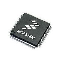
MCF51EM256CLL Freescale Semiconductor, MCF51EM256CLL Datasheet - Page 623

MCF51EM256CLL
Manufacturer Part Number
MCF51EM256CLL
Description
IC MCU 32BIT 256KB FLASH 100LQFP
Manufacturer
Freescale Semiconductor
Series
MCF51EMr
Datasheets
1.MCF51EM128CLL.pdf
(2 pages)
2.MCF51EM128CLL.pdf
(54 pages)
3.MCF51EM128CLL.pdf
(636 pages)
Specifications of MCF51EM256CLL
Core Processor
Coldfire V1
Core Size
32-Bit
Speed
50MHz
Connectivity
I²C, SCI, SPI
Peripherals
LCD, LVD, PWM, WDT
Number Of I /o
63
Program Memory Size
256KB (256K x 8)
Program Memory Type
FLASH
Ram Size
16K x 8
Voltage - Supply (vcc/vdd)
1.8 V ~ 3.6 V
Data Converters
A/D 16x12b
Oscillator Type
External
Operating Temperature
-40°C ~ 85°C
Package / Case
100-LQFP
Processor Series
MCF51EM
Core
ColdFire V1
Data Bus Width
32 bit
Data Ram Size
16 KB
Interface Type
RS-232, LIN
Maximum Clock Frequency
50 MHz
Number Of Timers
3
Operating Supply Voltage
1.8 V to 3.6 V
Maximum Operating Temperature
+ 85 C
Mounting Style
SMD/SMT
3rd Party Development Tools
JLINK-CF-BDM26, EWCF
Development Tools By Supplier
DEMOEM
Minimum Operating Temperature
- 40 C
Lead Free Status / RoHS Status
Lead free / RoHS Compliant
Eeprom Size
-
Lead Free Status / Rohs Status
Lead free / RoHS Compliant
Available stocks
Company
Part Number
Manufacturer
Quantity
Price
Company:
Part Number:
MCF51EM256CLL
Manufacturer:
FREESCALE
Quantity:
110
Company:
Part Number:
MCF51EM256CLL
Manufacturer:
Freescale Semiconductor
Quantity:
10 000
- Current page: 623 of 636
- Download datasheet (11Mb)
Multiple byte DDATA values are displayed in least-to-most-significant order. The processor captures only
those target addresses associated with taken branches that use a variant addressing mode (RTE and RTS
instructions, JMP and JSR instructions using address register indirect or indexed addressing modes, and
all exception vectors).
The simplest example of a branch instruction using a variant address is the compiled code for a C language
case statement. Typically, the evaluation of this statement uses the variable of an expression as an index
into a table of offsets, where each offset points to a unique case within the structure. For such
change-of-flow operations, the ColdFire processor loads the PSTB as follows:
Another example of a variant branch instruction is a JMP (A0) instruction.
entries that indicate a JMP (A0) execution, assuming CSR[BTB] was programmed to display the lower
two bytes of an address.
The PST of 0x05 indicates a taken branch and the marker value 0x0D indicates a 2-byte address.
Therefore, the following entries display the lower two bytes of address register A0, right-shifted by 1, in
least-to-most-significant nibble order. The next PST entry after the JMP instruction completes depends on
the target instruction. See
descriptions explaining the 2-bit prefix before each address nibble.
Freescale Semiconductor
1. Load PST=0x05 to identify that a taken branch is executed.
2. Optionally load the marker for the target address capture. Encodings 0x0D or 0x0E identify the
3. The new target address is optionally available in the PSTB. The number of bytes of the target
number of bytes loaded into the PSTB.
address loaded is configurable (2 or 3 bytes, where the encoding is 0x0D and 0x0E, respectively).
MCF51EM256 Series ColdFire Integrated Microcontroller Reference Manual, Rev. 8
Figure 26-24. Example JMP Instruction Output in PSTB
Section 26.4.3.2, “PST Trace Buffer (PSTB) Entry Format,”
{10, Address[16:13]}
PST/DDATA Values
{10, Address[12:9]}
{10, Address[4:1]}
{10, Address[8:5]}
0x0D
0x05
2-byte Address Marker
Taken Branch
Address >> 1
Description
Version 1 ColdFire Debug (CF1_DEBUG)
Figure 26-24
for entry
shows the PSTB
26-59
Related parts for MCF51EM256CLL
Image
Part Number
Description
Manufacturer
Datasheet
Request
R

Part Number:
Description:
BOARD DEMO HARDWARE ONLY
Manufacturer:
Freescale Semiconductor
Datasheet:

Part Number:
Description:
IC MCU 32BIT 128KB FLASH 100LQFP
Manufacturer:
Freescale Semiconductor
Datasheet:

Part Number:
Description:
IC MCU 32BIT 128KB FLASH 80LQFP
Manufacturer:
Freescale Semiconductor
Datasheet:

Part Number:
Description:
IC MCU 32BIT 256KB FLASH 80LQFP
Manufacturer:
Freescale Semiconductor
Datasheet:
Part Number:
Description:
Manufacturer:
Freescale Semiconductor, Inc
Datasheet:
Part Number:
Description:
Manufacturer:
Freescale Semiconductor, Inc
Datasheet:
Part Number:
Description:
Manufacturer:
Freescale Semiconductor, Inc
Datasheet:
Part Number:
Description:
Manufacturer:
Freescale Semiconductor, Inc
Datasheet:
Part Number:
Description:
Manufacturer:
Freescale Semiconductor, Inc
Datasheet:
Part Number:
Description:
Manufacturer:
Freescale Semiconductor, Inc
Datasheet:
Part Number:
Description:
Manufacturer:
Freescale Semiconductor, Inc
Datasheet:
Part Number:
Description:
Manufacturer:
Freescale Semiconductor, Inc
Datasheet:
Part Number:
Description:
Manufacturer:
Freescale Semiconductor, Inc
Datasheet:
Part Number:
Description:
Manufacturer:
Freescale Semiconductor, Inc
Datasheet:


