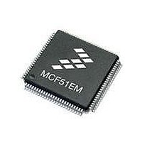
MCF51EM256CLL Freescale Semiconductor, MCF51EM256CLL Datasheet - Page 214

MCF51EM256CLL
Manufacturer Part Number
MCF51EM256CLL
Description
IC MCU 32BIT 256KB FLASH 100LQFP
Manufacturer
Freescale Semiconductor
Series
MCF51EMr
Datasheets
1.MCF51EM128CLL.pdf
(2 pages)
2.MCF51EM128CLL.pdf
(54 pages)
3.MCF51EM128CLL.pdf
(636 pages)
Specifications of MCF51EM256CLL
Core Processor
Coldfire V1
Core Size
32-Bit
Speed
50MHz
Connectivity
I²C, SCI, SPI
Peripherals
LCD, LVD, PWM, WDT
Number Of I /o
63
Program Memory Size
256KB (256K x 8)
Program Memory Type
FLASH
Ram Size
16K x 8
Voltage - Supply (vcc/vdd)
1.8 V ~ 3.6 V
Data Converters
A/D 16x12b
Oscillator Type
External
Operating Temperature
-40°C ~ 85°C
Package / Case
100-LQFP
Processor Series
MCF51EM
Core
ColdFire V1
Data Bus Width
32 bit
Data Ram Size
16 KB
Interface Type
RS-232, LIN
Maximum Clock Frequency
50 MHz
Number Of Timers
3
Operating Supply Voltage
1.8 V to 3.6 V
Maximum Operating Temperature
+ 85 C
Mounting Style
SMD/SMT
3rd Party Development Tools
JLINK-CF-BDM26, EWCF
Development Tools By Supplier
DEMOEM
Minimum Operating Temperature
- 40 C
Lead Free Status / RoHS Status
Lead free / RoHS Compliant
Eeprom Size
-
Lead Free Status / Rohs Status
Lead free / RoHS Compliant
Available stocks
Company
Part Number
Manufacturer
Quantity
Price
Company:
Part Number:
MCF51EM256CLL
Manufacturer:
FREESCALE
Quantity:
110
Company:
Part Number:
MCF51EM256CLL
Manufacturer:
Freescale Semiconductor
Quantity:
10 000
- Current page: 214 of 636
- Download datasheet (11Mb)
ColdFire Core
8.3.4
This section presents processor instruction execution times in terms of processor-core clock cycles. The
number of operand references for each instruction is enclosed in parentheses following the number of
processor clock cycles. Each timing entry is presented as C(R/W) where:
This section includes the assumptions concerning the timing values and the execution time details.
8.3.4.1
For the timing data presented in this section, these assumptions apply:
8-22
SRAMSZ
Field
•
•
1. The OEP is loaded with the opword and all required extension words at the beginning of each
2. The OEP does not experience any sequence-related pipeline stalls. The most common example of
3. The OEP completes all memory accesses without any stall conditions caused by the memory itself.
2–0
7–3
C is the number of processor clock cycles, including all applicable operand fetches and writes, and
all internal core cycles required to complete the instruction execution.
R/W is the number of operand reads (R) and writes (W) required by the instruction. An operation
performing a read-modify-write function is denoted as (1/1).
instruction execution. This implies that the OEP does not wait for the IFP to supply opwords and/or
extension words.
stall involves consecutive store operations, excluding the MOVEM instruction. For all STORE
operations (except MOVEM), certain hardware resources within the processor are marked as busy
for two clock cycles after the final decode and select/operand fetch cycle (DSOC) of the store
instruction. If a subsequent STORE instruction is encountered within this 2-cycle window, it is
stalled until the resource again becomes available. Thus, the maximum pipeline stall involving
consecutive STORE operations is two cycles. The MOVEM instruction uses a different set of
resources and this stall does not apply.
Thus, the timing details provided in this section assume that an infinite zero-wait state memory is
attached to the processor core.
SRAM bank size.
00000 No SRAM
00010 512 bytes
00100 1 KB
00110 2 KB
01000 4 KB
01010 8 KB
01100 16 KB (This is the value used for this device)
01111 24 KB
01110 32 KB
10000 64 KB
10010 128 KB
Else
Reserved.
Instruction Execution Timing
Table 8-11. D1 Hardware Configuration Information Field Description (continued)
Timing Assumptions
MCF51EM256 Series ColdFire Integrated Microcontroller Reference Manual, Rev. 8
Reserved for future use
Description
Freescale Semiconductor
Related parts for MCF51EM256CLL
Image
Part Number
Description
Manufacturer
Datasheet
Request
R

Part Number:
Description:
BOARD DEMO HARDWARE ONLY
Manufacturer:
Freescale Semiconductor
Datasheet:

Part Number:
Description:
IC MCU 32BIT 128KB FLASH 100LQFP
Manufacturer:
Freescale Semiconductor
Datasheet:

Part Number:
Description:
IC MCU 32BIT 128KB FLASH 80LQFP
Manufacturer:
Freescale Semiconductor
Datasheet:

Part Number:
Description:
IC MCU 32BIT 256KB FLASH 80LQFP
Manufacturer:
Freescale Semiconductor
Datasheet:
Part Number:
Description:
Manufacturer:
Freescale Semiconductor, Inc
Datasheet:
Part Number:
Description:
Manufacturer:
Freescale Semiconductor, Inc
Datasheet:
Part Number:
Description:
Manufacturer:
Freescale Semiconductor, Inc
Datasheet:
Part Number:
Description:
Manufacturer:
Freescale Semiconductor, Inc
Datasheet:
Part Number:
Description:
Manufacturer:
Freescale Semiconductor, Inc
Datasheet:
Part Number:
Description:
Manufacturer:
Freescale Semiconductor, Inc
Datasheet:
Part Number:
Description:
Manufacturer:
Freescale Semiconductor, Inc
Datasheet:
Part Number:
Description:
Manufacturer:
Freescale Semiconductor, Inc
Datasheet:
Part Number:
Description:
Manufacturer:
Freescale Semiconductor, Inc
Datasheet:
Part Number:
Description:
Manufacturer:
Freescale Semiconductor, Inc
Datasheet:


