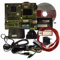
R0K572030S000BE Renesas Electronics America, R0K572030S000BE Datasheet - Page 845

R0K572030S000BE
Manufacturer Part Number
R0K572030S000BE
Description
KIT DEV FOR SH7203
Manufacturer
Renesas Electronics America
Series
Renesas Starter Kits (RSK)r
Type
MCUr
Specifications of R0K572030S000BE
Contents
CPU Board, LCD Module, E10A-Lite Emulator, Cable, QuickStart Guide and CD-ROM
Silicon Manufacturer
Renesas
Kit Contents
Board
Silicon Family Name
SH7203
Silicon Core Number
R5S72030W200FP
Tool / Board Applications
General Purpose MCU, MPU, DSP, DSC
Mcu Supported Families
SH7203
Lead Free Status / RoHS Status
Contains lead / RoHS non-compliant
For Use With/related Products
SH7203
Lead Free Status / Rohs Status
Compliant
- Current page: 845 of 1686
- Download datasheet (10Mb)
16.4.5
In SSU mode, data communications are performed via four lines: clock line (SSCK), data input
line (SSI or SSO), data output line (SSI or SSO), and chip select line (SCS).
In addition, the SSU supports bidirectional mode in which a single pin functions as data input and
data output lines.
(1)
Figure 16.4 shows an example of the initial settings in SSU mode. Before data transfer, clear both
the TE and RE bits in SSER to 0 to set the initial values.
Note: Before changing operating modes and communications formats, clear both the TE and RE
[1]
[2]
[3]
[4]
[5]
Initial Settings in SSU Mode
Clear the SSUMS bit in SSCRL to 0 and
Specify the MLS, CPOS, CPHS, CKS2,
Clear the TE and RE bits in SSER to 0
Set PFC for external pins to be used
bits to 0. Although clearing the TE bit to 0 sets the TDRE bit to 1, clearing the RE bit to 0
does not change the values of the RDRF and ORER bits and SSRDR. Those bits retain the
previous values.
and CEIE bits in SSER all together
CSS1, and CSS0 bits in SSCRH
specify bits DATS1 and DATS0
Specify TEIE, TIE, RIE, TE, RE
CKS1, and CKS0 bits in SSMR
SSU Mode
Specify the MSS, BIDE, SOL,
(SSCK, SSI, SSO, and SCS)
Start setting initial values
End
Figure 16.4 Example of Initial Settings in SSU Mode
[1] Make appropriate settings in the PFC for the external pins to be used.
[2] Specify master/slave mode selection, bidirectional mode enable,
[3] Selects SSU mode and specify transmit/receive data length.
[4] Specify MSB first/LSB first selection, clock polarity selection,
[5] Enables/disables interrupt request to the CPU.
SSO pin output value selection, SSCK pin selection, and SCS pin
selection.
clock phase selection, and transfer clock rate selection.
Section 16 Synchronous Serial Communication Unit (SSU)
Rev. 3.00 Sep. 28, 2009 Page 813 of 1650
REJ09B0313-0300
Related parts for R0K572030S000BE
Image
Part Number
Description
Manufacturer
Datasheet
Request
R

Part Number:
Description:
KIT STARTER FOR M16C/29
Manufacturer:
Renesas Electronics America
Datasheet:

Part Number:
Description:
KIT STARTER FOR R8C/2D
Manufacturer:
Renesas Electronics America
Datasheet:

Part Number:
Description:
R0K33062P STARTER KIT
Manufacturer:
Renesas Electronics America
Datasheet:

Part Number:
Description:
KIT STARTER FOR R8C/23 E8A
Manufacturer:
Renesas Electronics America
Datasheet:

Part Number:
Description:
KIT STARTER FOR R8C/25
Manufacturer:
Renesas Electronics America
Datasheet:

Part Number:
Description:
KIT STARTER H8S2456 SHARPE DSPLY
Manufacturer:
Renesas Electronics America
Datasheet:

Part Number:
Description:
KIT STARTER FOR R8C38C
Manufacturer:
Renesas Electronics America
Datasheet:

Part Number:
Description:
KIT STARTER FOR R8C35C
Manufacturer:
Renesas Electronics America
Datasheet:

Part Number:
Description:
KIT STARTER FOR R8CL3AC+LCD APPS
Manufacturer:
Renesas Electronics America
Datasheet:

Part Number:
Description:
KIT STARTER FOR RX610
Manufacturer:
Renesas Electronics America
Datasheet:

Part Number:
Description:
KIT STARTER FOR R32C/118
Manufacturer:
Renesas Electronics America
Datasheet:

Part Number:
Description:
KIT DEV RSK-R8C/26-29
Manufacturer:
Renesas Electronics America
Datasheet:

Part Number:
Description:
KIT STARTER FOR SH7124
Manufacturer:
Renesas Electronics America
Datasheet:

Part Number:
Description:
KIT STARTER FOR H8SX/1622
Manufacturer:
Renesas Electronics America
Datasheet:

Part Number:
Description:
KIT STARTER FOR R8C/18191A1B
Manufacturer:
Renesas Electronics America
Datasheet:


